Download
1 / 21
230 likes | 627 Views
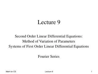
Lecture 9. OUTLINE pn Junction Diodes Electrostatics (step junction) Reading : Pierret 5; Hu 4.1-4.2. pn Junctions. A pn junction is typically fabricated by implanting or diffusing donor atoms into a p-type substrate to form an n-type layer:.

E N D
Lecture 9 OUTLINE • pn Junction Diodes • Electrostatics (step junction) Reading: Pierret 5; Hu 4.1-4.2
pn Junctions • A pn junction is typically fabricated by implanting or diffusing donor atoms into a p-type substrate to form an n-type layer: • A pn junction has a rectifying current-vs.-voltage characteristic: EE130/230M Spring 2013 Lecture 9, Slide 2
Terminology Doping Profile: EE130/230M Spring 2013 Lecture 9, Slide 3
Idealized pn Junctions • In the analysis going forward, we will consider only the net dopant concentration on each side of the pn junction: NA net acceptor doping on the p side: (NA-ND)p-side ND net donor doping on the n side: (ND-NA)n-side EE130/230M Spring 2013 Lecture 9, Slide 4
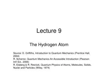
Electrostatics (Step Junction) Band diagram: Electrostatic potential: Electric field: Charge density: EE130/230M Spring 2013 Lecture 9, Slide 5
“Game Plan” to obtain r(x),E(x), V(x) • Find the built-in potential Vbi • Use the depletion approximation r (x) (depletion widths xp, xn unknown) • Integrate r (x) to find E(x) Apply boundary conditionsE(-xp)=0, E(xn)=0 • Integrate E(x) to obtain V(x) Apply boundary conditions V(-xp)=0, V(xn)=Vbi • For E(x) to be continuous at x=0, NAxp = NDxn Solve for xp, xn EE130/230M Spring 2013 Lecture 9, Slide 6
Built-In Potential Vbi For non-degenerately doped material: EE130/230M Spring 2013 Lecture 9, Slide 7
What if one side is degenerately doped? p+n junction n+p junction EE130/230M Spring 2013 Lecture 9, Slide 8
The Depletion Approximation In the depletion region on the p side, = –qNA In the depletion region on the n side, = qND EE130/230M Spring 2013 Lecture 9, Slide 9
Electric Field Distribution E(x) -xp xn x The electric field is continuous at x = 0 NAxp = NDxn EE130/230M Spring 2013 Lecture 9, Slide 10
Electrostatic Potential Distribution On the p side: Choose V(-xp) to be 0 V(xn) = Vbi On the n side: EE130/230M Spring 2013 Lecture 9, Slide 11
Derivation of Depletion Width • At x = 0, expressions for p side and n side must be equal: • We also know that NAxp = NDxn EE130/230M Spring 2013 Lecture 9, Slide 12
Depletion Width • Eliminating xp, we have: • Eliminating xn, we have: • Summing, we have: EE130/230M Spring 2013 Lecture 9, Slide 13
Depletion Width in a One-Sided Junction If NA >> NDas in a p+njunction: What about a n+p junction? where EE130/230M Spring 2013 Lecture 9, Slide 14
Peak E-Field in a One-Sided Junction EE130/230M Spring 2013 Lecture 10, Slide 15
V(x) in a One-Sided Junction p side n side EE130/230M Spring 2013 Lecture 9, Slide 16
Example: One-Sided pn Junction A p+n junction has NA=1020 cm-3 and ND =1017cm-3. Find (a) Vbi (b) W (c) xn and (d) xp. EE130/230M Spring 2013 Lecture 9, Slide 17
Voltage Drop across a pn Junction Note that VA should be significantly smaller than Vbi in order for low-level injection conditions to prevail in the quasi-neutral regions. EE130/230M Spring 2013 Lecture 9, Slide 18
Effect of Applied Voltage EE130/230M Spring 2013 Lecture 9, Slide 19
Summary • For a non-degenerately-doped pn junction: Built-in potential Depletion width • For a one-sided junction: Built-in potential Depletion width EE130/230M Spring 2013 Lecture 9, Slide 20
Linearly Graded pn Junction EE130/230M Spring 2013 Lecture 9, Slide 21