Download
1 / 2
20 likes | 35 Views
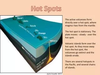
I<br>n this research, we present a novel method for visualising plasmonic `hot spots` upon plsmonic surfaces of gold nanostructures. Femtosecond laser pulses<br>have been used to map the locations of localised high<br>intensity electromagnetic fields i.e. the locations of<br>hot spots. Upon irradiation with 800 nm femtosecond laser pulses, which may be linearly or circularly polarised, it is possible to reveal the locations of<br>plasmonic hot spots since the nanostructures are<br>physically damaged i.e. undergo melting by the intense heat generated by femtosecond laser pulse<br>irradiation. SEM microscopy was used subsequently to map the surface of the nanostructures to show<br>which areas have been damaged, and hence reveal<br>the locations of the hot spots.

E N D
2020 Vol. 1, Iss. 1 Archives in Chemistry Extended Abstract Femtosecond Laser Irradiation for Hot Spots Mapping on the Surface of Plasmonic Nano- structures Nadia A. Abdulrahman Department of Chemistry, University of Baghdad, Baghdad, Iraq I es of gold nanostructures. Femtosecond laser pulses have been used to map the locations of localised high intensity electromagnetic fields i.e. the locations of hot spots. Upon irradiation with 800 nm femtosec- ond laser pulses, which may be linearly or circular- ly polarised, it is possible to reveal the locations of plasmonic hot spots since the nanostructures are physically damaged i.e. undergo melting by the in- tense heat generated by femtosecond laser pulse irradiation. SEM microscopy was used subsequent- ly to map the surface of the nanostructures to show which areas have been damaged, and hence reveal the locations of the hot spots. 2D arrays of quadric units (arranged in a racemic fashion) consisting of two patterns: gammadions and G-like shapes, have been used as plasmonic chiral nanostructures. It has been found that irradiation with linearly polarised light affected segments that are perpendicular to the polarisation direction of the incident beam. Howev- er, irradiation with circularly polarised light affected both horizontal and vertical segments of the nano- structures regardless the sense of individual features (i.e. left-handed or right-handed) or the sense of the circular polarisation of the incident beam (i.e. clock- wise or counter-clockwise). Hence, no enantio-selec- tivity was observed. n this research, we present a novel method for visu- alising plasmonic `hot spots` upon plsmonic surfac- significant degrees, encouraging the age of solid la- ser handle that are limited on the nanometer scale, consequently making ready for advancement meth- ods and advances. For instance, gold nanoparticles are being intended to search out destructive tumors in the body and, when lighted with a femtosecond laser, produce stun waves that pulverize the tumor with negligible harm to close by tissues. Also, a few fundamental tests have exhibited the capacity of la- ser-illuminated nanostructures to quicken electrons, recommending that nanomaterials may empower the manufacture of scaled down molecule quicken- ing agents. Nonetheless, changing these confirma- tion of-guideline ideas into handy advances requires a propelled comprehension of how nanostructures react to light fields that are close to the harm edge. For laser powers drawing closer and surpassing the harm edge (∼3 × 10¹³ W/cm2 for glass and gener- ally comparative for most other dielectric materi- als) the communication of femtosecond laser beats with mass materials is a perplexing procedure that is amazingly testing to demonstrate. The challenges stem to a great extent from the way that the laser beat adjusts the optical properties of the material on the femtosecond time scale, requiring a model that consolidates the properties of the laser field, the strong material, and the recently shaped plasma. Materials that show nanoscale structure present a further test since highlights littler than the frequen- cy of the light can upgrade the electric field on the nanometer scale, and this impact relies firmly upon the specific size, shape, and organization of the mol- ecule. For instance, past work outfit the capacity of nanostructured focuses to effectively ingest laser light to make splendid delicate X-beam sources, yet Introduction: The connection of solid (>1013 W/ cm2) laser fields with mass materials has far reach- ing applications, including exactness machining on the submicrometer scale, green union of nanopar- ticles and the creation of high-vitality electrons, particles, and photons. Nanoscale structures can locally upgrade a laser field, regularly by numerous
2020 Vol. 1, Iss. 1 Archives in Chemistry Extended Abstract the electromagnetic field dissemination around the Au nanorods, we performed limited contrast time- space (FDTD) reenactments (utilizing the FDTD ar- rangements programming bundle from Lumerical, Inc., Vancouver, Canada). In the reproductions, the elements of nanorods were picked as equivalent to the manufactured structures (95 nm×180 nm×40 nm), and the plane wave was episode onto the struc- tures at a rate point of 74°, which is indistinguishable from the PEEM tests. The optical properties of the gold were gotten utilizing the information from John- son and Christy. The TiO2 substrate was expected to act as a dielectric with a steady an incentive for the refractive file (n=2.6). The FDTD reproductions were performed on a discrete, non-consistently dis- persed work with a greatest goals of 2 nm. For the two planes, the figurings of the field power appro- priation are in acceptable concurrence with the test results acquired from the PEEM estimations with the full femtosecond laser beat excitation. The pinnacle improvement on the base plane was a lot more note- worthy than that on the top plane, as anticipated by the recreations. Be that as it may, approving this out- come utilizing the PEEM estimations is troublesome in light of the fact that the photoemissions from vari- ous vertical positions are hard to recognize. For most nanorods, the problem areas at the correct corners of the poles are more brilliant than those at the left corners. This wonder was additionally all around replicated by the reproductions and is credited to the hindrance effect33 in light of the fact that the light was illuminated from the left side at a touching point. Up until this point, the exceptionally spatially settled close field mapping of the LSPR field on the Au nanorods was effectively acquired with the PEEM estimations utilizing femtosecond laser beat light through nonlinear photoemission. As recently refer- enced, the frequency and abundancy of the LSPR rely upon the state of the nanostructures. the nitty gritty systems of this upgrade couldn’t be comprehended in detail in view of the unpredictabil- ity of the communication. In this manner, there is a squeezing requirement for new strategies that can give direct understanding into how nanomaterials collaborate with laser fields. Materials and methods: To manufacture the gold nanoparticle exhibits, we applied electron-pillar li- thography followed by metal faltering and lift-off methods. The creation strategy utilized in this inves- tigation was like the procedure depicted in our pre- vious reports. Examples of Au nanostructures were framed on Nb-doped TiO2 substrates that were struc- tured utilizing a high-goals electron-shaft lithography framework (ELS-F125; Elionix, Tokyo, Japan) working at kV. A regular copolymer oppose (ZEP520A; Zeon Chemicals, Louisville, USA) weakened with a ZEP more slender was turn covered onto the substrate at 1000 r.p.m. for 10 s and 4000 r.p.m. for 90 s, and it was then prebaked on a hot plate for 2 min at 150 °C. The electron-pillar lithography worked at an elec- trical flow of 3 nA. After turn of events, a 2-nm-thick titanium layer was first kept by means of faltering (MPS-4000; ULVAC, Tokyo, Japan) as the glue layer, trailed by a 40-nm-thick gold film. The lift-off was performed by progressively submerging the example in anisole, CH3)2CO and ultrapure water in a ultra- sonic shower. Four diversely formed Au nanoparticle clusters were used in this investigation, to be spe- cific, nanorods (rectangular), nanodisk-like particles (round), dimers and nanoblocks (square), and were organized in two-dimensional exhibits on the sub- strates. Field-outflow examining electron microscopy (JSM-6700FT; JEOL, Tokyo, Japan) and Fourier change infrared (FTIR) spectroscopy (FT/IR-6000TM-M; JAS- CO, Tokyo, Japan) were utilized to portray the mor- phologies and far-field unearthly properties of the Au nanostructures, separately. Results and discussion: To numerically ascertain