Download
1 / 24
240 likes | 375 Views
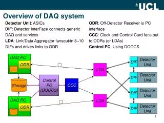
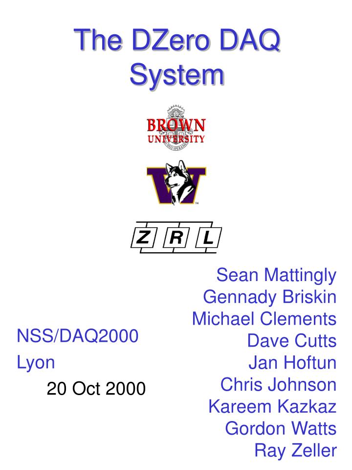
The DZero DAQ System. NSS/DAQ2000 Lyon 20 Oct 2000. Sean Mattingly Gennady Briskin Michael Clements Dave Cutts Jan Hoftun Chris Johnson Kareem Kazkaz Gordon Watts Ray Zeller. Detector. Trigger. Full. Readout. Information. DAQ. ~7 MHz. ~1 kHz. Level 1. Level 3. ~10 kHz.

E N D
The DZero DAQ System NSS/DAQ2000 Lyon 20 Oct 2000 Sean Mattingly Gennady Briskin Michael Clements Dave Cutts Jan Hoftun Chris Johnson Kareem Kazkaz Gordon Watts Ray Zeller
Detector Trigger Full Readout Information DAQ ~7 MHz ~1 kHz Level 1 Level 3 ~10 kHz ~50-70 Hz Level 2 C/R ~1 kHz Tape Output The DZero Trigger System Sean Mattingly Brown University - DZero
Data Acquisition Requirements in Run 2 • 60-80 readout crates • All crates -> 1 Farm Node for each event • ~800,000 readout channels • <250 KB> / event • Nominal Event Rate ~1 KHz • 250 MB/sec into DAQ/L3 Farm • Readout rate could approach 4 KHz with upgrades to digitizing electronics • With expansion DAQ can handle up to 10 KHz Sean Mattingly Brown University - DZero
Simplified Data Flow in L3/DAQ VME Buffer/Driver - in crate to be read out VBD VBD Readout Concentrator - collects data from up to 32 VBDs VRC Segment Bridge - routes data based on info from ETG SB ETG Event Tag Generator - receives event # and trigger bits from TF Node Level-3 filter node Configuration Control by L3Supervisor Sean Mattingly Brown University - DZero
SB SB Node Node Node Node Node Node Node Node SB SB Data Flow in L3/DAQ Data Collection Paths (8 * 2 * 48 MB/s) VBD VBD VBD o o o VRC Primary Fiber Paths (8 * 100 MB/s) (1 of 8) VBD VBD VBD o o o Level 1,2 Trigger Info ETG o o o • direct flow from VBD to Node • each data block flows freely and independently • blocks for different events flow simultaneously and asynchronously • recirculation loops allow maximum use of data path bandwidth • Segment Bridges use Event Tag data to perform complex realtime routing decisions event tag path o o o o o o o o o L3 data distribution to Level 3 farm Sean Mattingly Brown University - DZero
DAQ Architecture • Custom network modules hosted by commodity PCs • Unidirectional data flow • Simple communication setup • Each packet sent once • No packet loss • Data driven routing • Block header contains event number and crate identification • No communication w/ readout crates necessary • Data sender does not need to know where data needs to go • Routing based on L1/L2 trigger bits and node availability • No traffic shaping Sean Mattingly Brown University - DZero
DAQ Architecture • Recirculation loop • Flow Control • Back pressure • Near 100% utilization of bandwidth • No network load on CPU • Total Bandwidth = 800 MB/s • DAQ scalable beyond Run 2a needs Sean Mattingly Brown University - DZero
VME Buffer Driver (VBD) • Entry point of digitized data into DAQ • VBD receives 4-6 KB / event • Components: • VME interface with list processing DMA • Dual SRAM buffers • External data cable interface with token arbitration logic. • Performance: • VME: BLK mode DMA at 25-30 MB/sec • Data cable output: 48 MB/sec. • Token arbitration time: <10 micro sec. Readout Crate VBD Digitizers Digitizers Digitizers Token Control From last VBD or VRC Data Pathway 48 MB/sec To next VBD or VRC Sean Mattingly Brown University - DZero
DAQ Building Block:Serial Interface Buffer • VRC, SB, L3 Node, etc. all built from Serial Interface Buffer board(s) in a PC (Windows NT) • FPGA control • FPGA firmware changes for each application • Host PC can reprogram FPGAs via mapped local bus registers • Connections Available • High Speed Serial • Inova (1.32 Gb/s) • 1.32 Gb/s input AND output • Low Speed Serial • LVDS (50 MB/s) • VBD connection (VRC only) • FutureBus -> LVDS (48 MB/s) • PCI Sean Mattingly Brown University - DZero
Serial Interface Buffer Main Memory 128/256 MB SDRAM 72 bits wide Time sliced 10 ns clock Local Bus Control FPGA Altera APEX 200K
Serial Interface Buffer PCI Main Memory 128/256 MB SDRAM 72 bits wide Time sliced 10 ns clock Local Bus Control FPGA Altera APEX 200K Control CPU Intel i960RD 16 MB EDO RAM Host CPU
Serial Interface Buffer PCI Main Memory 128/256 MB SDRAM 72 bits wide Time sliced 10 ns clock Local Bus Control FPGA Altera APEX 200K Control CPU Intel i960RD 16 MB EDO RAM FIFO FIFO HS Serial Inova HS Serial Inova Host CPU 100 MB/s Fiber or Cu
Serial Interface Buffer PCI Main Memory 128/256 MB SDRAM 72 bits wide Time sliced 10 ns clock Local Bus Control FPGA Altera APEX 200K Control CPU Intel i960RD 16 MB EDO RAM FIFO FIFO LS Serial LVDS HS Serial Inova HS Serial Inova 50 MB/s Cu Host CPU 100 MB/s Fiber or Cu
Serial Interface Buffer VBD VBD VBD VBD PCI Future Bus Future Bus 48 MB/s Cu VRC Only LVDS LVDS FIFO FIFO VBD0 FPGA Altera 6024 VBD1 FPGA Altera 6024 Main Memory 128/256 MB SDRAM 72 bits wide Time sliced 10 ns clock Local Bus Control FPGA Altera APEX 200K Control CPU Intel i960RD 16 MB EDO RAM FIFO FIFO LS Serial LVDS HS Serial Inova HS Serial Inova 50 MB/s Cu Host CPU 100 MB/s Fiber or Cu
VBD VBD VBD VBD Inova Inova VBD Readout Collector (VRC) Data Cables 64cond / 26cond Serial Interface Buffer LVDS FIFO FutureBus -> LVDS FutureBus -> LVDS LVDS FIFO PCI Interface via i960 Connector Front Plate High Density Cable Optical Fiber Segment Bridges PC/PCI
VRC VRC VRC VRC VRC VRC VRC VRC Detailed DataFlow TF ETG Fiber Cable Interfaces ETI Segment Bridge Data Cable Interfaces Level 3 Interfaces Farm Nodes
Segment Bridge (SB) Event Tag Interface VRC/SB Firewire Low Voltage Differential Signal Inova LVDS/Lower Speed Inova Fiber PCI Interface via i960 SIB/FiberCable Interface Board PC/PCI SIB/Data Cable Interface Board PCI Interface via i960 Inova LVDS Copper ETI Nodes Firewire
To Trigger FrameWork • 128 Trigger Veto bits Event Tag Generator (ETG) From Trigger FrameWork Event Tag Creator (CAM Lookup) • 16 bit L3 Transfer Number • 128 Trigger Bits ET Queue Trigger Framework Interface Return ETG Monitor • Event Tag Format: • Header • Event Number • Flags (diagnostics or regular) • Segment Controller 1 Block • Event Type • FEC Readout Bit Masks • Segment Controller 2 Block • Event Type • FEC Readout Bit Masks • etc. SB SB SB SB Sean Mattingly Brown University - DZero
Inova Inova L3 Farm Node SB / Previous Node Next Node / ETI Copper • Farm Node communication • Token circulation from DCIs • Does not slow or clobber data flow • Nodes can asynch send READY to ETI • 36 bits of information • 32 bits data • 4 bits info/control • 4 L3 Interface Boards / Farm Node • 128 MB memory / board • Buffering for >1 Minute of 1KHz data taking PC/PCI PCI Interface via i960 SIB/L3 Interface Board
L3 Filter L3 Filter L3 Filter Process L3 Farm Node Control/ Monitoring Data Cables From SB PCI L3I 100-Base T Ethernet L3I Node-PCI I/O Module Control, Monitoring and Error Module L3I L3I Shared Memory Buffers L3 Node Framework Collector Router Module • 1000 Hz Farm input rate • Farm Output rate 50-70 Hz • Intel Based SMP System (4 Procs) • Windows 2000 • 1 L3 Filter Process per processor L3 Filter Interface Module Dedicated 100 Mbits/s Ethernet to Online Collector/Router Sean Mattingly Brown University - DZero
Outlook • Current Status • Full simulation (10 KHz with expansion) • Current Operation • DZero taking cosmics using low speed ethernet-based system • Driver for controlling SIB written • Simple control code using driver written • Final hardware soon to arrive • Test stand at Brown University ready • Monitoring and Control (see next talk) • On Track for First Collisions in March 2001 Sean Mattingly Brown University - DZero
Front End Token Readout Loop Front End Token Readout Loop Front End Crate Front End Crate Front End Crate Front End Crate VRC 1 VRC 8 Front End Crate Front End Crate Primary Fiber Channel Loop #8 Front End Crate Front End Crate Primary Fiber Channel Loop #1 SB 1 SB 4 L3 Node (1 of 16) L3 Node (1 of 16) Event Tag Loop Ethernet L3 Node (1 of 16) L3 Node (1 of 16) Ethernet ETG S (4 DATA CES L3 Node (1 of 16) L3 Node (1 of 16) To Collector Router To Collector Router Trigger Framework Segment Data Cables Segment Data Cables ) ) )
Dual Altera/FIFO FutureBus -> LVDS Altera FPGA 128 MB Memory Serial Interface Buffer (SIB) i960 Processor PC/PCI LVDS Lower Speed Serial Link Inova 1.32 Gb/s Full Duplex Serial Link