Download
1 / 18
180 likes | 377 Views
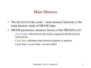
Lecture 13 Main Memory. Computer Architecture COE 501. Who Cares About the Memory Hierarchy?. Processor-DRAM Memory Gap (latency). µProc 60%/yr. (2X/1.5yr). 1000. CPU. “Moore’s Law”. 100. Processor-Memory Performance Gap: (grows 50% / year). Performance. 10. DRAM 9%/yr.

E N D
Lecture 13Main Memory Computer Architecture COE 501
Who Cares About the Memory Hierarchy? Processor-DRAM Memory Gap (latency) µProc 60%/yr. (2X/1.5yr) 1000 CPU “Moore’s Law” 100 Processor-Memory Performance Gap:(grows 50% / year) Performance 10 DRAM 9%/yr. (2X/10 yrs) DRAM 1 1980 1981 1982 1983 1984 1985 1986 1987 1988 1989 1990 1991 1992 1993 1994 1995 1996 1997 1998 1999 2000 Time
Impact on Performance • Suppose a processor executes at • Clock Rate = 200 MHz (5 ns per cycle) • CPI = 1.1 • 50% arith/logic, 30% ld/st, 20% control • Suppose that 10% of memory operations get 50 cycle miss penalty • CPI = ideal CPI + average stalls per instruction = 1.1(cyc) +( 0.30 (datamops/ins) x 0.10 (miss/datamop) x 50 (cycle/miss) ) = 1.1 cycle + 1.5 cycle = 2. 6 • 58 % of the time the processor is stalled waiting for memory! • a 1% instruction miss rate would add an additional 0.5 cycles to the CPI!
Main Memory Background • Performance of Main Memory: • Latency: Cache Miss Penalty • Access Time: time between request and when desired word arrives • Cycle Time: time between requests • Bandwidth: I/O & Large Block Miss Penalty (L2) • Main Memory is DRAM: Dynamic Random Access Memory • Dynamic since needs to be refreshed periodically (8 ms) • Addresses divided into 2 halves: • RAS or Row Access Strobe • CAS or Column Access Strobe • Cache uses SRAM: Static Random Access Memory • No refresh (6 transistors/bit vs. 1 transistor/bit for DRAM) • Address not divided • Size: DRAM/SRAM 4-8, Cost & Cycle time: SRAM/DRAM 8-16
Wr Driver & Precharger Wr Driver & Precharger Wr Driver & Precharger Wr Driver & Precharger - + - + - + - + - + - + - + - + Sense Amp Sense Amp Sense Amp Sense Amp Typical SRAM Organization: 16-word x 4-bit Din 3 Din 2 Din 1 Din 0 WrEn Precharge A0 Word 0 SRAM Cell SRAM Cell SRAM Cell SRAM Cell A1 Address Decoder A2 Word 1 SRAM Cell SRAM Cell SRAM Cell SRAM Cell A3 : : : : Word 15 SRAM Cell SRAM Cell SRAM Cell SRAM Cell Q: Which is longer: word line or bit line? Dout 3 Dout 2 Dout 1 Dout 0
A N 2 words N x M bit SRAM WE_L OE_L D M Logic Diagram of a Typical SRAM • Write Enable is usually active low (WE_L) • Bi-directional data • A new control signal, output enable (OE_L) is needed • WE_L is asserted (Low), OE_L is disasserted (High) • D serves as the data input pin • WE_L is disasserted (High), OE_L is asserted (Low) • D is the data output pin • Both WE_L and OE_L are asserted: • Result is unknown. Don’t do that!!!
Classical DRAM Organization (square) bit (data) lines r o w d e c o d e r Each intersection represents a 1-T DRAM Cell RAM Cell Array word (row) select Column Selector & I/O Circuits row address Column Address • Row and Column Address together: • Select 1 bit a time data
Logic Diagram of a Typical DRAM RAS_L CAS_L WE_L OE_L A 256K x 8 DRAM D 9 8 • Control Signals (RAS_L, CAS_L, WE_L, OE_L) are all active low • Din and Dout are combined (D): • WE_L is asserted (Low), OE_L is disasserted (High) • D serves as the data input pin • WE_L is disasserted (High), OE_L is asserted (Low) • D is the data output pin • Row and column addresses share the same pins (A) • RAS_L goes low: Pins A are latched in as row address • CAS_L goes low: Pins A are latched in as column address • RAS/CAS edge-sensitive
Main Memory Performance • Wide: • CPU/Mux 1 word; Mux/Cache, Bus, Memory N words (Alpha: 64 bits & 256 bits) • Interleaved: • CPU, Cache, Bus 1 word: Memory N Modules(4 Modules); example is word interleaved • Simple: • CPU, Cache, Bus, Memory same width (32 bits)
Main Memory Performance Cycle Time Access Time Time • DRAM (Read/Write) Cycle Time >> DRAM (Read/Write) Access Time • 2:1; why? • DRAM (Read/Write) Cycle Time : • How frequent can you initiate an access? • Analogy: A little kid can only ask his father for money on Saturday • DRAM (Read/Write) Access Time: • How quickly will you get what you want once you initiate an access? • Analogy: As soon as he asks, his father will give him the money • DRAM Bandwidth Limitation analogy: • What happens if he runs out of money on Wednesday?
Increasing Bandwidth - Interleaving Access Pattern without Interleaving: CPU Memory D1 available Start Access for D1 Start Access for D2 Memory Bank 0 Access Pattern with 4-way Interleaving: Memory Bank 1 CPU Memory Bank 2 Memory Bank 3 Access Bank 1 Access Bank 0 Access Bank 2 Access Bank 3 We can Access Bank 0 again
address address address address 0 1 4 5 2 3 9 8 6 7 12 13 10 11 14 15 Bank 1 Bank 0 Bank 2 Bank 3 Main Memory Performance(Figure 5.32, pg. 432) • How long does it take to send 4 words? • Timing model • 1 cycle to send address, • 6 cycles to access data + 1 cycle to send data • Cache Block is 4 words • Simple Mem. = 4 x (1+6+1) = 32 • Wide Mem. = 1 + 6 + 1 = 8 • Interleaved Mem. = 1 + 6 + 4x1 = 11
Wider vs. Interleaved Memory • Wider memory • Cost for the wider connection • Need a multiplexor between cache and CPU • May lead to significantly larger/more expensive memory • Intervleaved memory • Send address to several banks simultaneously • Want Number of banks > Number of clocks to access bank • As the size of memory chips increases, it becomes difficult to interleave memory • Difficult to expand memory by small amounts • May not work well for non-sequential accesses
Avoiding Bank Conflicts • Lots of banks int x[256][512]; for (j = 0; j < 512; j = j+1) for (i = 0; i < 256; i = i+1) x[i][j] = 2 * x[i][j]; • Even with 128 banks their are conflicts, since 512 is an even multiple of 128 • SW: loop interchange or declaring array not power of 2 • HW: Prime number of banks • bank number = address mod number of banks • address within bank = address / number of banks • modulo & divide per memory access? • address within bank = address mod number words in bank (3, 7, 31)
N cols RAS_L Page Mode DRAM: Motivation Column Address • Regular DRAM Organization: • N rows x N column x M-bit • Read & Write M-bit at a time • Each M-bit access requiresa RAS / CAS cycle • Fast Page Mode DRAM • N x M “register” to save a row DRAM Row Address N rows M bits M-bit Output 1st M-bit Access 2nd M-bit Access CAS_L A Row Address Col Address Junk Row Address Col Address Junk
N cols Fast Page Mode Operation Column Address • Fast Page Mode DRAM • N x M “SRAM” to save a row • After a row is read into the register • Only CAS is needed to access other M-bit blocks on that row • RAS_L remains asserted while CAS_L is toggled DRAM Row Address N rows N x M “SRAM” M bits M-bit Output 1st M-bit Access 2nd M-bit 3rd M-bit 4th M-bit RAS_L CAS_L A Row Address Col Address Col Address Col Address Col Address
Fast Memory Systems: DRAM specific • Multiple column accesses: page mode • DRAM buffers a row of bits inside the DRAM for column access (e.g., 16 Kbits row for 64 Mbits DRAM) • Allow repeated column access without another row access • 64 Mbit DRAM: cycle time = 90 ns, optimized access = 25 ns • New DRAMs: what will they cost, will they survive? • Synchronous DRAM: Provide a clock signal to DRAM, transfer synchronous to system clock • RAMBUS: startup company; reinvent DRAM interface • Each chip a module vs. slice of memory • Short bus between CPU and chips • Does own refresh • Variable amount of data returned • 1 byte / 2 ns (500 MB/s per chip) • Niche memory or main memory? • e.g., Video RAM for frame buffers, DRAM + fast serial output
Main Memory Summary • Wider Memory • Interleaved Memory: for sequential or independent accesses • Avoiding bank conflicts: SW & HW • DRAM specific optimizations: page mode & Specialty DRAM