Download
1 / 28
280 likes | 295 Views
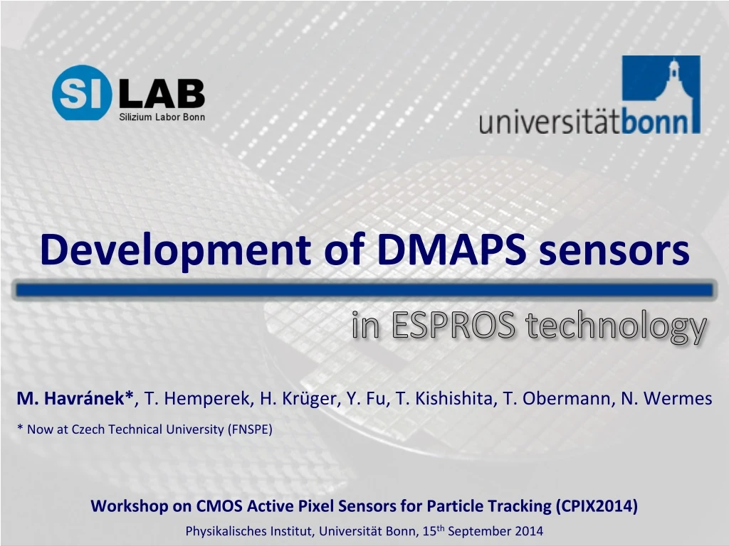
Development of DMAPS sensors. in ESPROS technology. M. Havránek * , T. Hemperek , H. Krüger , Y. Fu, T. Kishishita , T. Obermann , N. Wermes * Now at Czech Technical University (FNSPE). Workshop on CMOS Active Pixel Sensors for Particle Tracking (CPIX2014).

E N D
Development of DMAPS sensors in ESPROS technology M. Havránek*, T. Hemperek, H. Krüger, Y. Fu, T. Kishishita, T. Obermann, N. Wermes * Now at Czech Technical University (FNSPE) Workshop on CMOS Active Pixel Sensors for Particle Tracking (CPIX2014) PhysikalischesInstitut, Universität Bonn, 15th September 2014
Sensor requirements for particle tracking • General requirements • Minimize multiple scattering to increase momentum resolution • => low mass (thinned) sensors needed • Granularity (currently 400×50 resp. 250×50 µm2 (IBL)) • Sufficient signal to noise ratio (hybrid pixels ≈ 100) • Radiation hardness (≈ 100 Mrad) • Low power (3.5 mW/mm2 for innermost layer (RD53)) • => in case of 50x50 µm2 pixels we need 8.75 µW/pixel Multiple scattering • Monolithic pixels • High granularity (small pixels) • Low mass (thinned sensor) possible • One chip – no bump-bonding – fast prototyping • Large SNR – questionable • Potentially low cost solution for large area tracker • Complex electronics in pixel – questionable • Radiation hardness - questionable
Depleted Monolithic Active Pixel Sensor • Existing MAPS technologies: • - standard CMOS MAPS, HV MAPS, • epi-layer MAPS, INMAPS, T3 MAPS ….. • - not all of them suitable for HEP • experiments • Problem of the “standard” MAPS • - slow and incomplete charge collection • - not full CMOS in pixel • - limited radiation hardness Epi-layer based MAPS Depleted MAPS • Depleted MAPS – non-standard CMOS process • - large signal from depleted bulk • - possibility to integrate full CMOS • - enhanced radiation tolerance • - even thin sensor can provide good SNR
ESPROS - technology for DMAPS fabrication • Technology options needed • - High resistive substrate • - High voltage (≈10 V) • - Quadruple well • Advantages w.r. to standard CMOS MAPS • - Large signal (theoretically 4 ke-/MIP • at 50 µm thick silicon substrate) • - Fast charge collection • - Potentially high radiation hardness • ESPROS Photonic Process • - 150 nm CMOS process • - Near IR sensors • - 1.8 V domain • - 6 metal layers
Test chip – EPCB01 • Test-chip submitted in late 2012 • - chip size 1.4×1.4 mm2 • - six different DMAPS pixel matrices • - thinned down to 50 µm • - 8×8 and 6×8 matrix dimension DMAPS • Chip output • - configuration and read-out with a shift register • - each matrix (except V4) has analog output from • one pixel
DMAPS pixel DMAPS pixel layout • Complex CMOS electronics in pixel • - 160-180 transistor per pixel • - Pixel size 40×40 µm2 • - Sensitive electrode ≈20×20µm2 (depends what • we include) Custom design electrode (V2,V5) • High voltage domain (≈10V) Low voltage domain (1.8 V) • Two sensor biasing options: • - biasing with a diode • - biasing with a resistor
DMAPS pixel variants Variants of DMAPS matrices • Explore potential of DMAPS pixels • - six matrix variants • - different sensor geometry • - different biasing options • - different front-end architectures
Tests done with EPCB01 • Initial testing, configurability, response to radioactive sources • Testing with charge injection, gain, noise • Cluster size measurement with 90Sr • Gain determination with 55Fe • More detailed characterization (laser scan, beam test . . .) will be presented in: • ESPROS DMAPS: Results and Radiation Hardness • by Theresa Obermann • on Wednesday at 16:30
First tests DMAPS response to radiation Mean = 1782 ADU Sigma = 36.7 ADU 1 ADU = 0.2 x 0.637 mV 50 mV Sigma ~ 40 e- 300 mV Detector is alive!! Injection of various signal charge V3 – DC coupling V2 – diode biasing V1 – resistor biasing Observation nr. 1: DMAPS pixels respond to signal (injection and irrad.) but each pixel version gives different amplitude
Response to charge injection V1 - continuous FE, EPC sens. (AC*, RB*) V2 - continuous FE, custom sens. (AC, DB**) V3 - continuous FE, custom sens. (DC*) V5 – switched FE, custom sens. (AC, DB) V6 – switched FE, EPC sens. (AC, RB) • Linearity measured with threshold • scan (threshold = 50% hits) • Dispersion between channels: • - threshold • - gain * AC/DC – coupling between sensor electrode and FE ** RB/DB – resistor or diode biased sensor electrode
Gain and noise Gain of FE electronics determined by charge injection Noise of FE electronics determined by charge injection Error bars reduced 2x Error bars reduced 2x • V2 – best performance: gain ≈ 100 µV/e-; noise ≈ 30e- • V1, V2 – identical FE but different gain – WHY? V1 => Most likely due to different capacitance of the Sensitive electrode IDENTICAL LAYOUT V2 If open loop gain a is small, the closed loop gain of the CSA can be altered by sensor capacitance Cd
Signal and noise of DMAPS pixels Large noise superimposed on signal (500 e-) V3 – DC coupling V1 – resistor biasing V2 – diode biasing • Excessive noise observed by oscilloscope • Present in all DMAPS variants • Random telegraph noise • Can be caused by too small transistors
Threshold tuning • Untuned chip has large threshold fluctuations TDAC in V1-V3: All versions – 352 channels V2 = ch224-ch287 • Tuning helps to reduce fluctuations in all versions All versions – 352 channels TDAC in V4-V6: Pixels out of tunable range V2 = ch224-ch287
Cluster size Sr90 occurence HV_BIAS = 11 V cluster size • Threshold set to 1 ke- and tuned • Mostly single and double pixel clusters • Long tail due to soft component of energy spectrum of Sr90 • How the clusters change if we change bias voltage ??
Cluster size - bias voltage effects occurence occurence HV_BIAS = 11 V HV_BIAS = 8 V cluster size cluster size occurence occurence HV_BIAS = 5 V HV_BIAS = 2 V cluster size cluster size
Cluster size - bias voltage effects HV_BIAS [V] HV_BIAS [V] • Number of hits almost constant at HV_BIAS > 3 V • Average cluster size increases with bias voltage • Single hit / double hit clusters decreases • with HV_BIAS and saturates at 6 V (full depletion) HV_BIAS [V]
Gain determination with Fe55 • DMAPS channel – single bit resolution • Differentiating threshold scan we can get spectrum • Enormous statistics needed: • - data collection ~ 10 days • - reconstructed spectrum at every pixel: Fe55
Gain comparison V2 (injection VS source scan) • Gain from source scan is 34 % higher • than determined by charge injection • Gain variations between channels • almost match in both cases • Systematic shift can be explained by • increasing input capacitance when charge • injection is enabled → gain decreases • (see next slide) • Determination of error bars: • 1.) Q injection method: uncertainty of injection capacitance 10 % (≈ typical process variation) • 2.) 55Fe source scan: error (1 std. dev.) comes from coarse binning of 55Fe spectrum to see the peak
Capacitance of MOSCAP Explanation of gain difference • Situation 1 (charge injected from sensor side): • When SW is ON, CSA sees higher input capacitance by ≈ 1 fF reducing gain when injection is enabled • Since capacitance of input transistor is 0.62 fF the additional capacitance of 1fF is significant • Simulation test – gain measured by both methods • Situation 2 (charge injected with injection circuit):
Lessons learned with EPCB01 • General remarks • - Concept of DMAPS pixels works – but FE electronics needs improvements!! • - Open loop gain of CSA needs to be large (at least several hundreds) • - Closed loop gain has to be carefully adjusted by additional feedback • capacitance (1-2 fF) • - Use larger transistors to reduce danger of RTS noise • Designers remarks: • => every 100 aF capacitance matters!! • => optimize routing of the CSA to minimize parasitic capacitances • => design carefully injection circuit not to add too much parasitic capacitance • => post-layout simulation and understanding influence of parasitics is important
EPCB02 • EPCB02 is evolution of EPCB01 • - cascode amplifier with high open loop gain • - added 2 fF feedback capacitor -> uniformity • - both charge collection electrodes are custom • - input transistors are larger • - each pixel has analog output • (multiplexed → unity gain buffer → IO pad) D2 D1 • EPCB02 will allow to study independently: V1 vs V2 – effects of biasing (RB/DB) V1 vs V4 – cont. vs switched FE V4 vs V5 – different sensor geom. V4 vs V6 – different transistor size
Circuit for capacitance measurement in EPCB02 • Various layouts and biasing circuits can influence sensor capacitance • Cd is important parameter for rise-time and noise optimization • Charge-pump based circuit for capacitance measurement of DMAPS sensor • Two transistor charge pump: • - CV measurement => depl. voltage. • - compare different geometries
Conclusions • EPCB01 demonstrator of DMAPS sensor in ESPROS technology • - Depletion voltage ≈ 6 V (based on cluster size saturation) • - Gain variation between pixels ≈ 20 %, significant threshold dispersion • - RTS noise • - New chip EPCB02 will allow more detailed studies of DMAPS pixels • Open questions for applications in HEP: • - Radiation hardness and effects of radiation damage • - How to integrate complex digital logic (ToT, trigger logic, SEU latches …..)?
Signal rise-time • Rise-time => 25% - 75% signal amplitude • Upper limit on charge collection time Irradiation with 90Sr cut on 2.7-3.3 ke- events trise =19.5 ns Charge injection of 3 ke- trise =14.2 ns • Fast charge collection • 50 % of the signal charge is collected for less than 19.5 ns
X-ray irradiation X-ray irradiation End-point energy 60 keV Doses: 200 krad – 50 Mrad Annealing: 100 min @ 80 oC Tests: threshold scan w/wo charge injection of 2ke -> fitting S-curve -> threshold -> gain and ENC extraction digital test: shift in / shift out data patterns: 0000…, 111…, 10101… discharge curves of the CSA IV-curves of the sensor 10 cm
Radiation effects • Small radiation effects in analog FE: • - small changes of gain and noise • - pulse shortening • No effect on digital logic at all
Radiation effects - transistors Measured by L. Germic • Threshold voltage shift of all transistors • gm degradation – mostly affects PMOS – narrow channel