Download
1 / 16
210 likes | 493 Views
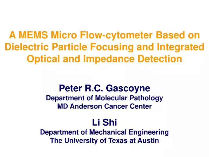
A MEMS Micro Flow-cytometer Based on Dielectric Particle Focusing and Integrated Optical and Impedance Detection. Peter R.C. Gascoyne Department of Molecular Pathology MD Anderson Cancer Center Li Shi Department of Mechanical Engineering The University of Texas at Austin. Flow Cytometry.

E N D
A MEMS Micro Flow-cytometer Based on Dielectric Particle Focusing and Integrated Optical and Impedance Detection Peter R.C. GascoyneDepartment of Molecular PathologyMD Anderson Cancer CenterLi ShiDepartment of Mechanical EngineeringThe University of Texas at Austin
Flow Cytometry • Capability • Measures physical and chemical properties of single cells or other biological particles as they flow in fluid stream past a light source • Analyze 105 cells per second • Applications • Analysis of blood cells, bacteria, nuclei, chromosomes • Detection of cancer cells – labeling of surface markers • Measurement of particle size, shape, granularity, etc. • Sort cells
Injector Tip Sheath fluid Fluorescence signals Focused laser beam Basics of Flow Cytometry Hydrodynamic Focusing Purdue University Cytometry Laboratories • Focus cells in suspension by sheath fluid • Illuminate cells in the focused suspension stream • Analyze cells by detecting scattered and fluorescence light
Positive dielectrophoresis Principle of Dielectrophoresis
Negative dielectrophoresis Principle of Dielectrophoresis
Dielectrophoretic Particle Focusing DEP forces can be used to focus, trap or repel particles, enabling particle fractionation and separation Fringing fields at electrode edges provide DEP levitation forces in direction normal to the electrode plane
Design of the DEP focusing channel Use negative DEP to focus cells in the central region of the stream Integrate fluorescent and impedance detectors into flow channel
Electrode Fabrication Top View of the Bottom Electrodes Bus bars to provide AC electric field of 90 phase difference, i.e. 0, 90,180, 270. Bus Bar Channel Side View Electrode
Electrode Fabrication(Cont’d) Deposit inter-metal dielectrics, etch holes 2 1 Deposit gold electrodes Si Substrate 3 Fabricate similar electrodes on a glass wafer Deposit and pattern gold layer and insulation layer 4 Glass substrate Same phase of the electric field
Electrode Fabrication(Cont’d) 5 Deposit SU-8, pattern a channel SU-8 channel Bonding process to complete the channel Side View 6 Glass SU-8 Si
Optical Detector Fabrication Fiber coupled to a blue LED A Glass wafer TiO2/SiO2 multilayer interference filter SU8 Au/Ti contact pads P-Si Channel p-n diode A A-A Side View Flow in Flow out
Acknowledgement • BME Seed Grant • Graduate Student: Choongho Yu, UT Austin