Download
1 / 26
260 likes | 587 Views
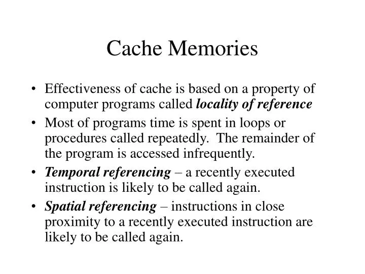
Cache Memories. Effectiveness of cache is based on a property of computer programs called locality of reference Most of programs time is spent in loops or procedures called repeatedly. The remainder of the program is accessed infrequently.

E N D
Cache Memories • Effectiveness of cache is based on a property of computer programs called locality of reference • Most of programs time is spent in loops or procedures called repeatedly. The remainder of the program is accessed infrequently. • Temporal referencing – a recently executed instruction is likely to be called again. • Spatial referencing – instructions in close proximity to a recently executed instruction are likely to be called again.
Cache Memories • Based on locality of reference • Temporal • Recently executed instructions are likely to executed again soon • Spatial • Instructions in close proximity to a recently executed instruction (with respect to an address) are also likely to be executed soon. • Cache Block – a set of contiguous address locations (cache block = cache line)
Conceptual Operation of Cache • Memory control circuitry is designed to take advantage of locality of reference. • Temporal – • Whenever an information (instruction or data) is first needed, this item should be brought into the cache where it will hopefully remain until it is needed again. • Spatial – • Instead of fetching just one item from the main memory to the cache, it is useful to fetch several items that reside at adjacent addresses well. • A set of contiguous addresses are called a block • cache block or cache line
Cache Memories • Using an example cache size of 128 blocks of 16 words each. (total of 2048 – 2K words) • Main memory is addressable by a 16-bit address bus (64K words – viewed as 4K blocks of 16 words each)
Write through Protocol • Cache and main memory are updated simultaneously • Write Back Protocol • Update on the cache and mark it with an associated flag bit (dirty or modified bit) • Main memory is updated later, when the block containing this marked word is to be removed from cache to make room for a new block.
Write Protocols • Write through • Simpler, but results in unnecessary Write operations in main memory when a cache word is updated several times during its cache residency. • write back • can result in unnecessary write operations because when a cache block is written back to the memory all words of the block are written back, even if only a single word has been changed while the block was in the cache.
Mapping Algorithms • Processor does not need to know explicitly that there is a cache. • Based on R/W operations, the cache control circuitry determines whether the requested word currently exists in the cache. (Hit) • If information is in cache for a read, main memory is not involved. For write operations, system can either use write-through protocol or write-back protocol
Mapping Functions • Specification of correspondence between the main memory blocks and those in cache. • Hit or Miss • Write through Protocol • Write back protocol (uses dirty bit) • Read miss • Load through or early restart on read miss • Write Miss
Read Protocols • Read miss • Addressed word is not in cache • Block of words containing requested word is written from main memory to cache. • After entire block is written to cache, particular word is forwarded to processor. Or word may be sent to processor as soon as it is read from main memory (load-through or early-restart) reduces processor’s wait time but requires more complex circuitry.
Write Miss • If addressed word is not in cache for a write operation, write miss occurs. • write-through • information is written directly into main memory. • Write-back • block containing word is brought into cache, then the desired word in the cache is overwritten with the new information.
Mapping Functions Cache Block 0 tag Cache consists of 128 blocks of 16 words each, total of 2048 (2K words) tag Block 1 tag Block 127
Main Memory Block 0 Block 1 Main memory hasx 64K words, viewed as 4K blocks of 16 words each Block 127 Block 128 Block 129 Tag Block Word 5 7 4 Block 255 Main memory address Block 256 Block 257 Block 4095
Direct Mapping • Block J maps to Block J modulo 128 of the cache • Main memory blocks 0, 128, 256, … map to block 0 of cache • Blocks 1, 129, 257, … map to block 1 • … • Contention can arise for the position even if the cache is not full. • Contention resolved by allowing new block to overwrite the currently resident block
Placement of block in Cache • Direct mapping - easy to implement – not very flexible. • Determined from memory address • Low-order 4 bits select one of 16 words in a block • When a new block enters cache, 7-bit block field determines cache position • 5-bit high order are stored in tag address. They identify which of the 32 blocks that are mapped to this position are currently resident. Tag Block Word 5 7 4 Main memory address
Associative Mapping • Much more flexible – higher costs (must search all 128 tag patterns to determine if a given block is in cache. • All tags must be searched in parallel • A main memory block can be placed into any cache block position. • Existing blocks only need to be ejected if cache is full. Tag Word 12 4 Main memory address
Set Associative Mapping • Blocks of cache are grouped into sets • A block of main memory can reside in any block of a specific set. • Reduces contention problem of direct mapped; reduces hardware necessary for searching tag addresses as seen in associative mapped. • K-blocks per set is a k-way set associative cache Tag Set Word 6 6 4 Main memory address
Valid Bit • Provided for each block • Indicates whether the block contains valid data • Not the same as dirty bit (used with the write-through method) which indicated whether the block has been modified during its cache residency. • Transfers from disk to main memory are normally handled with DMA transfers, bypassing cache for both cost and performance reasons. • Valid bit is set to 1 first time loaded into cache from main memory. Whenever a main memory block is updated by a source that bypasses cache, checks are meade to determine if block being loaded is in cache. If it is, valid bit is cleared to 0.
Cache Coherence • Also, before a DMA transfer, need to determine if information in main memory is up-to-date with information in cache. (write back protocol) • One solution is to always flush the cache by forcing the dirty data to be written back to memory before a DMA transfer takes place.
Replacement Algorithms • Direct mapped • No replacement algorithm necessary – position of each block is predetermined. • When cache is full, what block(s) must be ejected. • LRU – least recently used replacement • Overwrite the block that has gone the longest time without being referenced. • Cache controller must keep records of all references to all blocks. • Algorithm performs well for many access patterns • Poor performance when accesses are made to sequential elements of an array that is slightly too large to fit in the cache.
Caches in Commercial Processors • 68040 Caches • 2 caches (each 4K bytes) (1 instruction, 1 data) • Uses set associative organization (64 sets, each 4 blocks) • Each block has 4 long words, each long word 4 bytes.
Caches in Commercial ProcessorsPentium III (high performance processor) • Requires fast access to instructions and data • 2 cache levels • Level 1 – • 16KB instruction • 2-way set-associative organization (instructions not normally modified during execution) • 16KB data • 4-way set associative organization • Can use either writeback or write through policy • Level 2 • Much larger
Level 2 Cache of Pentium III • Can be implemented external to processor • Katmai • 512KB • Implemented using SRAM memory • 4-way set-associative organization • Uses either write-back or write through protocol, programmable on a per-block basis. • Cache bus is 64-bits wide
Level 2 Cache of Pentium III • Can be integrated with processor • Coppermine • 256KB • 8-way set-associative organization • Cache bus is 256-bits wide
Which method is better? • External cache • allows larger cache • Larger data path width not available because of pins needed and increased power consumption of output drivers • Has slower clock speeds (Katmai driven at half processor speed; coppermine driven at full processor speed) • Internal cache • Reduces latency, increases bandwidth because of wider path • Processor chip becomes much larger, making it much more difficult to fabricate.
Pentium 4 Caches • Can have up to 3 levels of cache • L1 • Data cache (8 Kbytes) • 4-way set-associative organization • Cache block 64K bytes • Write through policy is used on writes • Integer data can be accessed from data cache in 2 clock cycles (less than 2 ns) • Instruction cache does not hold normal instructions (rather already decoded versions of instructions).
L2 of Pentium 4 Unified cache of 256K bytes 8-way set-associative Write-back policy Access latency is 7 clock cycles Implemented on processor chip. L3 cache also available for on-chip but not for desktops, intended for servers.