Download
1 / 32
330 likes | 539 Views
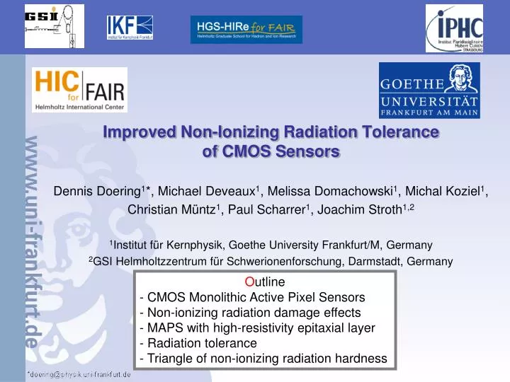
Improved Non- Ionizing Radiation Tolerance of CMOS Sensors Dennis Doering 1 *, Michael Deveaux 1 , Melissa Domachowski 1 , Michal Koziel 1 , Christian Müntz 1 , Paul Scharrer 1 , Joachim Stroth 1,2 1 Institut für Kernphysik, Goethe University Frankfurt/M, Germany

E N D
Improved Non-Ionizing Radiation Tolerance of CMOS Sensors Dennis Doering1*, Michael Deveaux1, Melissa Domachowski1, Michal Koziel1, Christian Müntz1, Paul Scharrer1, Joachim Stroth1,2 1Institut für Kernphysik, Goethe University Frankfurt/M, Germany 2GSI Helmholtzzentrum für Schwerionenforschung, Darmstadt, Germany • Outline • CMOS MonolithicActive Pixel Sensors • Non-ionizingradiationdamageeffects • MAPS withhigh-resistivityepitaxiallayer • Radiation tolerance • Triangleof non-ionizingradiationhardness
CMOS Monolithic Active Pixel Sensors • Used by industry (digital camera) • Have been modified for charged particle detection since 1999 by IPHC Strasbourg • Foreseen for STAR, CBM, ALICE, ILC… => Sharing of R&D costs. Current compromise Optimized for one parameter Dennis Doering: Improved Non-Ionizing Radiation tolerance of CMOS sensors RESMDD Florence Oct 2012
Design of a MAPS 10-40 µm => a few µm resolution N+ 50 µm SiO2 P-Well N+ P+ Sensingdiode P- Epitaxial Layer Substrate P+ ~50 µm thinsensors ⇒ Low material budget High granularity ⇒ Goodspatialresolution Dennis Doering: Improved Non-Ionizing Radiation tolerance of CMOS sensors RESMDD Florence Oct 2012
Charge spectrum Diode Epitaxial Layer Particle e- e- Dennis Doering: Improved Non-Ionizing Radiation tolerance of CMOS sensors RESMDD Florence Oct 2012
Non-ionizingradiationdamageeffect Diode Epitaxial Layer Defects due to radiation Particle Charge losses due torecombinationatradiation-induceddefects e- Dennis Doering: Improved Non-Ionizing Radiation tolerance of CMOS sensors RESMDD Florence Oct 2012
Influenceofradiationdamageandpixelpitch Large pixelpitch Large pixelpitch Diode Epitaxial Layer Defects due toradiation Small pixelpitch Small pixelpitch Diode Epitaxial Layer e- e- Dennis Doering: Improved Non-Ionizing Radiation tolerance of CMOS sensors RESMDD Florence Oct 2012
Pixel pitcheffect In mostofthecases, thewholechargecanbedetected. Little lossesfor larger pixelpitchevenunirradiated Dennis Doering: Improved Non-Ionizing Radiation tolerance of CMOS sensors RESMDD Florence Oct 2012
Pixel pitcheffect Signal lossesdepend on thepixelpitch. Dennis Doering: Improved Non-Ionizing Radiation tolerance of CMOS sensors RESMDD Florence Oct 2012
Pixel pitcheffect Smallerpixelpitchimprovesradiationtolerance. Drawback: NumberofpixelReadout time Power consumption Dennis Doering: Improved Non-Ionizing Radiation tolerance of CMOS sensors RESMDD Florence Oct 2012
High-resistivity New CMOS processavailable: High-resistivity: Decreaseofdopingconcentration in epitaxiallayer. Low-resistivity ~ 30 Ωcm High-resistivity ~1k Ωcm Sensingdiode SiO2 depletedvolume P-Well N+ P+ P- Epitaxial Layer Substrate P+ • Larger depletedvolumes: • ⇒ Acceleratedchargecollection • ⇒ Improved non-ionizingradiationtolerance Dennis Doering: Improved Non-Ionizing Radiation tolerance of CMOS sensors RESMDD Florence Oct 2012
MIMOSA-18 AHR MIMOSA-18 AHR: Analog sensorwithhigh-resistivityEpitaxial Layer. Main features: High-resistivity ~1k Ωcm EPI layer 2.5V-3V depletionvoltage Pixel pitchfrom 25µm down to 10µm Irradiation upto 3·1014neq/cm² @ TRIGA reactor (Ljubljana/Slovenia) Dennis Doering: Improved Non-Ionizing Radiation tolerance of CMOS sensors RESMDD Florence Oct 2012
Signal response MIP-likeβ (Ru-106) Seedpixel More drift, less diffusion: ⇒Signal charge focused to seed pixel ⇒Signal amplitude doubled Dennis Doering: Improved Non-Ionizing Radiation tolerance of CMOS sensors RESMDD Florence Oct 2012
Signal response MIP-likeβ (Ru-106) Seedpixel Radiation damageeffect after 3·1014neq/cm² : Signal losses due torecombinationsobserved. However, theirradiatedhigh-resistivitysensorexhibits a highersignalamplitudethantheunirradiatedlow-resistivitysensor. Dennis Doering: Improved Non-Ionizing Radiation tolerance of CMOS sensors RESMDD Florence Oct 2012
Noise Radiation damage Substantial increase in thebulknoiseisobserved. Dennis Doering: Improved Non-Ionizing Radiation tolerance of CMOS sensors RESMDD Florence Oct 2012
Noise Radiation damage Useoftemperaturedependenceofbulknoise Dennis Doering: Improved Non-Ionizing Radiation tolerance of CMOS sensors RESMDD Florence Oct 2012
Noise Cooling Radiation damage Noise isalleviatedto a factorof 2 withdecreasingtemperature. Expect further noise reduction in case of faster readout. Dennis Doering: Improved Non-Ionizing Radiation tolerance of CMOS sensors RESMDD Florence Oct 2012
Signal to Noise ratio S/N limit (MIPS) Dennis Doering: Improved Non-Ionizing Radiation tolerance of CMOS sensors RESMDD Florence Oct 2012
Signal to Noise ratio (High-resistivity) S/N limit (MIPS) Error bars: Fit uncertainty + 10% noiseuncertainty Dennis Doering: Improved Non-Ionizing Radiation tolerance of CMOS sensors RESMDD Florence Oct 2012
Signal to Noise ratio High-resistivity S/N limit (MIPS) Error bars: Fit uncertainty + 10% noiseuncertainty Dennis Doering: Improved Non-Ionizing Radiation tolerance of CMOS sensors RESMDD Florence Oct 2012
Signal to Noise ratio High-resistivity S/N limit (MIPS) Error bars: Fit uncertainty + 10% noiseuncertainty Dennis Doering: Improved Non-Ionizing Radiation tolerance of CMOS sensors RESMDD Florence Oct 2012
Radiation tolerance Dennis Doering: Improved Non-Ionizing Radiation tolerance of CMOS sensors RESMDD Florence Oct 2012
Summary • Radiation tolerance studies up to 3·1014neq/cm² • Results: • CMOS sensors based on high-resistivity epitaxial layer exhibit substantially improved performance, (S/N ~ doubled) • Radiation tolerancedepends on thepixelpitch • Laboratory test indicates: • Radiation tolerance is beyond 3·1014neq/cm² (Pitch 10µm, cooled sensor) • Outlook: • Ionizing radiation hardness addressed by MIMOSA-32 – fabricated in an 0.18µm process -> S. Senyukov (next talk) Dennis Doering: Improved Non-Ionizing Radiation tolerance of CMOS sensors RESMDD Florence Oct 2012
Triangle of non-ionizing radiation tolerant MAPS Resistivity Temperature Pitch Dennis Doering: Improved Non-Ionizing Radiation tolerance of CMOS sensors RESMDD Florence Oct 2012
BACKUP Dennis Doering: Improved Non-Ionizing Radiation tolerance of CMOS sensors RESMDD Florence Oct 2012
Radiation tolerance Sensor: - Mi-18 AHR, SB-Pixel, 10 µm pitch - Epitaxiallayer: 400 W cm, 15 µm Irradiation: - fast reactorneutrons (Triga, Ljubljana) - Chip not poweredduringirradiation - Dose: 3 · 1014neq/cm² + O(3 MRad) Gain ok 3 · 1014neq/cm² + O(3 MRad) Not irradiated CCE ok Noise increases => Compensatewithcooling. Noise increases <20% lessentries Thinneractive vol.? Fe-55 (X-rays) Ru-106 (b-rays) 490e (MPV) <20% lesssignal Thinneract. vol.? 620e (MPV) 99% det. eff. after irrad. Preliminaryconclusion: Sensor tolerates 3 · 1014neq/cm², tobeconfirmed in beam test Dennis Doering: Improved Non-Ionizing Radiation tolerance of CMOS sensors RESMDD Florence Oct 2012
Pixel with 12µm and 25µm pitch (Fe-55) Seedpixelcluster MIMOSA-18 AHR 12µm (A1) MIMOSA-18 AHR 25µm (A2) Fe-55 X-ray CCE shifted CCE ok gain ok 12 µm pitch: Average CCE isconstant. 25µm pitch: Shifttolowervaluesasobserved in sensorsbased on lowresistivity EPI layer. Dennis Doering: Improved Non-Ionizing Radiation tolerance of CMOS sensors RESMDD Florence Oct 2012
Pixel with 12µm and 25µm pitch (Fe-55) Cluster of 25 pixel => Larger diffusionpaths 12 µm pitch: Shiftofclusterpeaknowvisible ⇒ somesignalcharges lost which diffuse longerdistance (toneighborpixels) 25µm pitch: Dramaticshift ⇒ 12µm pixelpitch: in a partofEpitaxiallayersignal lost due torecombinationcanbeneglected Dennis Doering: Improved Non-Ionizing Radiation tolerance of CMOS sensors RESMDD Florence Oct 2012
Temperaturemeasurementwithinfraredcamera Huber system CC 815 -70°C - + 35°C Infrared MIMOSA-18 Sensor isoperating Camerapaint T ofsensor T ofcooling liquid -3°C /-20°C Dennis Doering: Improved Non-Ionizing Radiation tolerance of CMOS sensors RESMDD Florence Oct 2012
High resistivity Standard: 13 Ω cm; NA≈1015 cm-3 High resistivity: 400 Ω cm; NA≈3.3 1013 cm-3 Size ofthe depletedzone Doping concentration • Idea: Decreasingthedopingconcentrationfrom 1015shouldincreasethesizeofthedepletedzone: • Improvedperformanceexpected. Dennis Doering: Improved Non-Ionizing Radiation tolerance of CMOS sensors RESMDD Florence Oct 2012
Applicationsof MAPS STAR-Experiment CBM-Experiment (FAIR, GSI) Possible ITS-Upgrade ALICE International Linear Collider MAPS are developed for applications as vertex detector since 1999 at IPHC (Strasbourg). Dennis Doering: Improved Non-Ionizing Radiation tolerance of CMOS sensors RESMDD Florence Oct 2012
MIMOSA-26 - Working horse since several years Pixel column Sensingpart • 21.2 x 10.6 mm² 1152 discriminators Digital part zero suppr. logic On-chip voltage regulators JTAG slow control Output memories Read out time: ~100 µs => ~ 10k frames/second Radiation tolerance: >300 kRad; > Dennis Doering: Improved Non-Ionizing Radiation tolerance of CMOS sensors RESMDD Florence Oct 2012
Pixel pitcheffect Photons (Fe-55) Summedclustercharge Signal lossesdepend on thepixelpitch. Dennis Doering: Improved Non-Ionizing Radiation tolerance of CMOS sensors RESMDD Florence Oct 2012