Download
1 / 21
210 likes | 241 Views
Explore how FPGA's and Modulator/PhotoDetector Arrays mimic various forms of OCDMA, with matched filtering in time and spectral domains. Learn about Equivalence Between Spectral Phase Encoding and Time Sequential Encoding, and more.

E N D
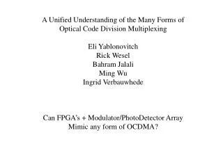
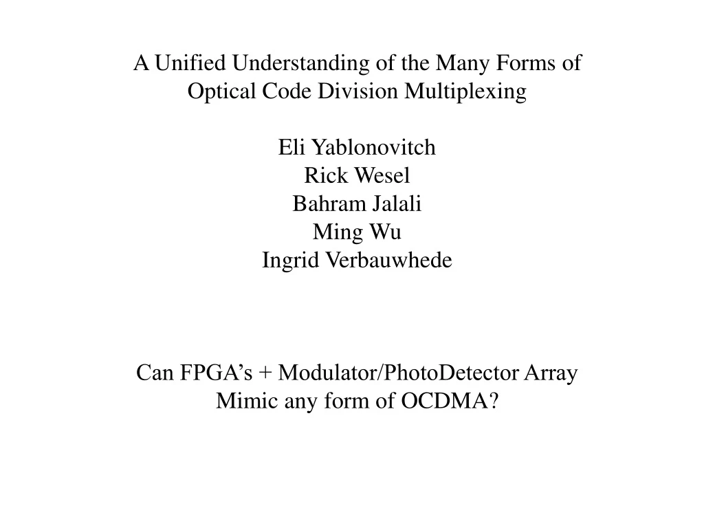
A Unified Understanding of the Many Forms of Optical Code Division Multiplexing Eli Yablonovitch Rick Wesel Bahram Jalali Ming Wu Ingrid Verbauwhede Can FPGA’s + Modulator/PhotoDetector Array Mimic any form of OCDMA?
Matched Filtering in Time Domain (non-coherent) Princeton USC UC Davis Telcordia Purdue Univ. Matched Filtering in the Spectral Domain (coherent)
l1 l1 l2 l2 Wavelength l3 Wavelength l3 l4 l4 Time Time Time DWDM MUX DWDM DEMUX Modulators Threshold Level (valid data) FPGA Voltage Photodetectors Time Block Diagram To Network Multi-wavelength Laser Source Transmitter Data FPGA Code Wavelength Receiver Data From Network
FPGA Encryption System clock PLL LVDS Input Protocol LVDS Output Switch Matrix Output clock Input clock Input data Output data Delay Module Code Generator LVDS: Low Voltage Differential Signaling PLL: Phase-Locked Loop
Therefore FPGA’s + Modulator/PhotoDetector Array can easily duplicate the performance of Matched Filtering in Time Domain (non-coherent) Therefore Princeton scheme and USC scheme can be emulated by our FPGA approach
Equivalence Between Spectral Phase Encoding And Time Sequential Encoding: (a) (a) Sequential brief individual pulses, have a broad spectrum as indicated by the colors. The plus and minus signs in (a) indicate various phase shifts induced on the spectral components of one pulse. The phase shifts can be decoded by a matched filter, producing a single big pulse that can be monitored by a threshold detector. (b) • With no loss of generality, the pulses can be spectrally filtered, and each spectral component • sent to a phase sensitive photo-receiver. The retrieved information can be stored and processed • in a Field Programmable Gate Array, which is fully equivalent to direct-sequence radio CDMA.
Figure 1: Coherent detection without a local oscillator. The ring is a carrier add/drop separation filter.
Figure 4: Tandem single side band receiver, not requiring a local oscillator, avoids duplicate side-bands.
Direct Sequence Spread Spectrum: A Direct Sequence radio CDMA system imposes random phase shifts +1 or –1 on the signals in much the same way as the channelized optical spectral phase decoder/encoder, described in a previous vugraph.
Therefore FPGA’s + Modulator/PhotoDetector Array can do Spectral Phase Encoding if Coherent detectors are used Therefore UC Davis scheme and Telcordia scheme and Purdue scheme can be emulated by our FPGA approach
The different approaches are all equivalent since, the frequency time rectangular cell changes shape, but its area is preserved, in accordance with the “Uncertainty Principle”. Conventional Wavelength/Time matrix. Frequency and time are treated on an equal footing. Spectral Phase Encoding. Each color of each pulse will be coded with a different phase shift, producing narrow slicing of the spectrum, but relatively long periods between pulses. Direct-Sequence Time-Domain Spread-Spectrum CDMA. Each channel occupies a broad frequency spectrum corresponding to the inverse of the chip time.
Successive Decoding • We can decode the first user by treating others as noise, then the first user’s ones become erasures for the other users. Proceed in this way until finish decoding all the users. • This is called successive decoding. For binary OR channel, this process does not lose capacity as compared to joint decoding.
Successive Decoding: The Z-Channel • Successive decoding for n users: • User with lowest rate is decoded first • Other users are treated as noise • The decoded data of the first user is used in the decoding of the remaining users • First user sees a “Z-channel” • Where ai=1-(1-p)n-i is the probability that at least one of the n-i remaining users transmits a 1
Simple codes • In order to have a hardware demo working for the May meeting, some very simple codes were produced. • This demo consists of two transmitter and two receivers • Both receivers decode the information independently
Simple Codes for Demo • Short codes have been designed for a simple demo for 2 users • These were chosen to be as simple to encode and decode as possible • Each bit is encoded separately • Bit synchronism is assumed, blocked asynchronism is allowed • Coordination is required • These codes are error free
Simple codes for Demo (2) 1 Rate 1/4 0 0 Source 2 Source 1 1 1 2 3 4 1 2 3 4 5 6 Rate 1/6 0 1 Receiver 1 looks for position of 0 (which always exists) If 1 or 2, decide 1 If 3 or 4, decide 0 Sum Rate 5/12 Receiver 2 looks for FIRST position of 0. If 1, 3 or 5, decide 1 If 2, 4 or 6, decide 0 Worst Case : block i block i+1
FPGA FPGA FPGA Decoder Decoder Encoder Encoder Modulator Modulator Bit Error Rate Tester Bit Error Rate Tester Data Generator Data Generator CW Laser CW Laser Photodetector Photodetector FPGA Setup for initial successive decoding Demo Transmitter 1 Receiver 1 Wavelength Coupler Transmitter 2 FPGA Receiver 2