Download
1 / 22
220 likes | 326 Views
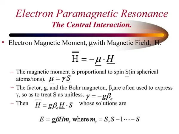
Electron EDM Measurement using a Paramagnetic Crystal. Chen-Yu Liu and S. Lamoreaux (P-23) M. Espy and A. Matlachov (P-21). 6/2/03. Shapiro’s proposal. Usp. Fiz. Nauk., 95 145(1968). High Z material high high net eEDM. E field aligns eEDM eEDM // eSpin.

E N D
Electron EDM Measurement using a Paramagnetic Crystal Chen-Yu Liu and S. Lamoreaux (P-23) M. Espy and A. Matlachov (P-21) 6/2/03
Shapiro’s proposal Usp. Fiz. Nauk., 95 145(1968) • High Z material high high net eEDM. • E field aligns eEDM • eEDM // eSpin. • Induces bulk magnetization, which produces B flux. • Reverse the E field, and the magnetization signal is modulated.
Figure of Merit • Induced flux: • Paramagnetic susceptibility: • Large density of paramagnetic sites. • Low temperature. • Large unit magnetic moment: • Enhancement factor: • Large A (for =AB). • Effective field: • Large K. • E*=Eext/3
What’s required? • High E field Sample with • A small conductivity. • A high dielectric strength. • A large dielectric constant to reduce D cancellation. • Large magnetic response. An insulating paramagnet. • Sensitive magnetometer • SQUID. • Optical method? • Non-linear Faraday effect in atomic vapors.
Features of solid state eEDM exp. • No effect. • High number density of bare electrons. • Solid state: • High dielectric strength. • Large magnetic response. • Concerns • Parasitic, hysteresis effects.
First solid state eEDM exp. B.V. Vasil’ev and E.V. Kolycheva, Sov. Phys. JETP, 47 [2] 243 (1978) • Sample: Nickel Zinc ferrite • dielectric strength ~ 2kV/cm. • Fe3+: b = 4 B . (uncompensated moment) • Atomic enhancement factor = 0.52. • Magnetic permeability = 11 (at 4.2K). (m=0.8) • Electric permittivity =2.20.2. (=0K) • Cubic lattice. • No magnetoelectric effect. • Sample size: 1cm in dia., 1mm in height. (0.08 c.c.) • E Field: 1Kv/cm, 30Hz reversal rate • Temperature : 4.2K • rfSQUID with a field sensitivity of 10-16 T. • dFe3+= (4.26.0) 10-23 e-cm de=(8.1 11.6)10-23 e-cm
New Version • Gd3+ in GGG • 4f75d06s0 ( 7 unpaired electrons). • Atomic enhancement factor = -2.20.5. • Langevin paramagnet. • Dielectric constant ~ 12. • Low electrical conductivity and high dielectric strength • Volume resistivity = 1016-cm. • Dielectric strength = 10 MV/cm for amorphous sample. (Crystalline sample tend to have lower K) • Cubic lattice. • Larger sample: 100 c.c. (4cm in dia. 2 cm in height 2 pieces) • Higher E field: 5-10kV/cm. • Lower temperature ~ 50mK (with a DR). • Better SQUID design. • V.A. Dzuba et al., xxx.lanl.gov:physics/020647 (June 2002)
Solid State Properties of GGG • Gadolinium Gallium Garnet • Gd3Ga5O12 • Garnet Structure: {A3}[B2](C3)O12 • A {dodecahedron}: M3 • Ca, Mn, Fe, R (La,..Gd,..Lu) • B [octahedron],C (tetrahedron): • Fe, Ga, … • Ceramic of good electrical properties.
Bake GGG Polycrystal K. McClellan in MST-8 • Solid State Reaction of the Oxides E.E. Hellstrom et al., J. Am. Ceram. Soc., 72 1376 (1989) • Weigh powders of 3 (Gd2O3):5 (Ga2O3) mole ratio, dried at 1000C for 9 h in air. • Mixed and ball-milled with Zirconia balls and acetone in polyethylene jars for 6 h. • Dry in air to remove acetone. • Isostatically pressed into a pellet, then prereact at 1350C for 6 h in air in high-purity alumina crucibles. • Crush the prereacted pellet using agate mortar and pestle and ball-milled (as before) for 24 h. • Cold press the powder into pellets, and sinter at 1650C for 10 h. • Heating and cooling rates: 200C/h below 1000C 100C/h above 1000C
Alumina Crucible Parallel plate capacitor Single crystal GGG Polycrystal GGG
20 30 40 50 60 70 80 90 X-ray diffraction of GGG J. Valdez and K. Sickafus in MST-8 5/30/03 Polycrystal crushed powder Polycrystal bulk surface Single crystal crushed powder 2
Magnetic Properties of GGG • Gd3+: half filled 4f orbital • 7 e- (spin aligned) • L=0, S=7/2 {A3}[B2](C3)O12 • Spin: {} [] () • JAB<0, JAC>0, JBC<0 • |JAA|,| JAB| << |JAC| • In A sublattice: • JAA<0 (AF coupling) • JNN S(S+1) ~ 1.5K • Geometrically frustrated AF magnet: Spin glass transition at 0.4K. (Limit of temperature)
Susceptibility m Measurement I Sample magnetization: M=mH= m(Hext+Hm) = m(B0/0-fM)
Susceptibility m Measurement II • Sample disk toroid, inductance • Resonant frequency: • Width of the resonant peak: || B(1+C/T) 1.31K 4K 70K 4% change
Electrical Properties of Poly-GGG V0 • Dielectric constant • K ~ 10-20 • Leakage current Vm
Instrumentation • Macor/graphite coated electrodes. (reduce Johnson noise) • Sample/electrode plates sandwiched by G10 clamps. • G10 can wrapped by superconducting Pb foils (two layers). • Rectangular magnetic field formed by high Metglas alloy ribbons. • Additional layers of “cryoperm 10” sheets. • A magnetic shielding factor > 109. • The whole assembly is immersed in L-He bath, cooled by a high cooling power dilution refrigerator. (10W at 10mK, 100W at 100mK)
Magnetic flux pick-up coil (planar gradiometer) • Common rejection of residual external • uniform B field and fluctuations. • Enhancement of sample flux pick-up. + R1=2cm R2=2.2cm R3=(R12+R22)=3.42cm LG=700nH for 10m dia. wire =500nH for 100m dia. Wire (Nb superconducting wire) 0 _ 2.5” 5”
SQUID M. Espy and A. Matlachov • DC SQUID: two Josephson junctions on a superconducting ring. • Flux to voltage transformer. • Energy sensitivity ~ 5 at 50 mK. • Flux noise ~ 0.2 0/√Hz. • Field sensitivity: in principle can be infinite by using large pick-up coil with thin wire, typically fT/√Hz. • Pick-up coil connects to a spiral SQUID input coil, which is inductively coupled to SQUID. • Coupling constant (geometrical factor)?
How well can we do? • Lsq= 0.2 nH (intrinsic) • Lp=0.7 H (gradiometer) • Li=0.5 H • Coupling eff. = sq/p = √(LsqLi)/(Lp+Li)= 810-3. • de = sq/sq=(0.20/√t)/(810-3 p) • with 10kV/cm, T=10mK, A=100 cm2 around GGG • p =170 per 10-27e-cm • de = 1.4710-27 /√te-cm • In 10 days of averaging, de~ 10-30 e-cm.
Expected systematic effects • Random noise: • High voltage fluctuation. • SQUID 1/f noise. • Sample 1/f noise, due to paramagnetic dissipation. ??? • External B field fluctuation. (gradiometer) • Displacement current at field reversal. • Generate large field. (position of the pick-up coil) • Too big a field change for SQUID to follow. ??? • Leakage current. (<10-14A, should be feasible at low temp.) • Linear magneto-electric effect. • Deviation from cubic symmetry. ??? • Vibrations relative to the superconducting Pb can (trapped flux field fluctuations). ??? • Magnetic impurities. (no problem, as long as they don’t move.) • Spin-lattice relaxation ??? • Energy dissipation < 10W at 10mK.
Tentative Schedule (√ ) Sample preparation and characterization. (fall 2002) (√ ) Design and build experiment. (spring 2003) ( _ ) Couple to dilution refrigerator. (fall 2003) ( _ ) First measurement using SQUID. (winter 2003) ( _ ) Preliminary results. (spring 2004) ( _ ) Improved version using optical method. (summer 2004)