Download
1 / 13
130 likes | 253 Views
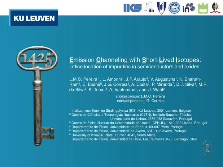
E mission C hanneling with S hort- L ived I sotopes: lattice location of impurities in semiconductors and oxides.

E N D
Emission Channeling with Short-Lived Isotopes: lattice location of impurities in semiconductors and oxides L.M.C. Pereira1, L. Amorim1, J.P. Araújo4, V. Augustyns1, K. Bharuth-Ram6, E. Bosne5, J.G. Correia2, A. Costa2, P. Miranda7, D.J. Silva4, M.R. da Silva3, K. Temst1, A. Vantomme1, and U. Wahl2 spokesperson: L.M.C. Pereira contact person: J.G. Correia 1 Instituut voor Kern- en Stralingsfysica (IKS), KU Leuven, 3001 Leuven, Belgium 2 Centro de Ciências e Tecnologias Nucleares (C2TN), Instituto Superior Técnico, Universidade de Lisboa, 2686-953 Sacavém, Portugal 3 Centro de Física Nuclear da Universidade de Lisboa (CFNUL), 1649-003 Lisboa, Portugal 4 Departamento de Física, Universidade do Porto, 4169-007 Porto, Portugal 5 Departamento de Física, Universidade de Aveiro, 3810-193 Aveiro, Portugal 6 University of KwaZulu Natal, Durban 4041, South Africa 7 Departamento de Física, Universidad de Chile, Las Palmeras 3425, Santiago, Chile
motivation and outline Latticelocationexperimentsonsemiconductors and oxides of fundamental and technological relevance • Transition metals in dilute magnetic semiconductors isotopes: 56Mn (t1/2=2.6 h), 59Fe (45 d), 61Co (1.6 h) and 65Ni (2.5 h) • p-type dopants in nitride semiconductors isotopes: 27Mg (9.5 min) and 11Be (13.8 s) • Positron emitter 11C (20.4 min) for β+ emission channeling (feasibility) Part of a wide research program involving complementary large-scale facility techniques • Synchrotron radiation • Neutron scattering L.M.C. Pereira, INTC meeting, CERN, 25.10.2013
emission channeling technique - decay, CE electron yield angle
emission channeling technique electron yield electron yield L.M.C. Pereira, INTC meeting, CERN, 25.10.2013 angle
emission channeling technique Newsletter of the Faculty of Science - KU Leuven (Sept.-Nov. 2013) L.M.C. Pereira, INTC meeting, CERN, 25.10.2013
dilutemagneticsemiconductors (DMS) “Classic” DMS • Mn-dopednarrow-gap III-Vs (GaAs, InAs, …) Key question:interstitial Mn site-change and migration Experiments: low-T 56Mn in Ga1-xMnxAs (Nottingham) previousworkonthelowconcentrationregime: L.M.C Pereira et al., Appl. Phys. Lett. 98, 201905 (2011) L.M.C Pereira et al., Phys. Rev. B 86, 125206 (2012) L.M.C. Pereira, INTC meeting, CERN, 25.10.2013
dilutemagneticsemiconductors (DMS) “Classic” DMS • Mn-dopednarrow-gap III-Vs (GaAs, InAs, …) Key question:interstitial Mn site change and migration Experiments: low-T 56Mn in Ga1-xMnxAs (Nottingham) • TM-dopedwide-gap oxides and nitrides (ZnO, GaN,…) Key question: anion substitutional TMs: why/how? Experiments: 56Mn/ 59Fe in Mn/Fe-doped GaN and Al1-xGaxN (Linz) L.M.C. Pereira, INTC meeting, CERN, 25.10.2013
dilutemagneticsemiconductors (DMS) “Classic” DMS • Mn-dopednarrow-gap III-Vs (GaAs, InAs, …) Key question:interstitial Mn site change and migration Experiments: low-T 56Mn in Ga1-xMnxAs (Nottingham) • TM-dopedwide-gap oxides and nitrides (ZnO, GaN,…) Key question: anion substitutional TMs: why/how? Experiments: 56Mn/ 59Fe in Mn/Fe-doped GaN and Al1-xGaxN (Linz) previousworkonthelowconcentrationregime: L.M.C Pereira et al., Phys. Rev. B 84, 125204 (2011) L.M.C Pereira et al., Phys. Rev. B 86, 195202 (2012) L.M.C Pereira et al., Appl. Phys. Lett. 103, 091905 (2013) L.M.C. Pereira, INTC meeting, CERN, 25.10.2013
dilutemagneticsemiconductors (DMS) “Novel” DMS • Transition metal dopedternary oxides Key question:single-ionferromagnetism Experiments: 56Mn/59Fe/61Co/65Ni in SrTiO3, LiNbO3… Theory: G. F. Dionne (MIT) X-rayabsorption fine structure Nuclear resonantscattering X-raymagnetic circular dichroism Synchrotronradiaction X-raydiffraction Polarizedneutronreflectivty Fe in displaced Ti sites in Sr(Fe,Ti)O3 Fe in ideal Ti sites in Sr(Fe,Ti)O3 undoped SrTiO3 L.M.C. Pereira, INTC meeting, CERN, 25.10.2013
p-typedopants in nitrides • 27Mg and 11Be in GaN, AlN, InN Key questions:preciselatticelocation of acceptors and therelationtoholelocalization and self-compensation Experiments: 27Mg: higher angular resolution low-temperature 11Be: new isotope ourpreviouswork (27Mg:GaN/AlN): L.M. Amorimet al., submittedtoPhys. Rev. Lett. L.M. Amorimet al., submittedtoAppl. Phys. Lett. J.L. Lyons et al., Phys. Rev. Lett. 108, 156403 (2012) L.M.C. Pereira, INTC meeting, CERN, 25.10.2013
p-typedopants in nitrides • 27Mg and 11Be in GaN, AlN, InN Key questions:preciselatticelocation of acceptors and therelationtoholelocalization and self-compensation Experiments: 27Mg: higher angular resolution low-temperature 11Be: new isotope feasibility 11Be:GaN L.M.C. Pereira, INTC meeting, CERN, 25.10.2013
11C β+ emission channeling • Case-studyforpositronemission channeling • Relevantfor: • Dopant/contaminant in semiconductors/metals • Graphene growth (e.g. C-implanted Ni) • Implantationdamage and annealing in SiC and diamond • … Expected positron blocking patterns from substitutional 11C in Si at room temperature for 11C16O+ implantation with 50 keV. L.M.C. Pereira, INTC meeting, CERN, 25.10.2013
beamrequest Total requestedshifts: 30 L.M.C. Pereira, INTC meeting, CERN, 25.10.2013