Download
1 / 33
360 likes | 1.17k Views
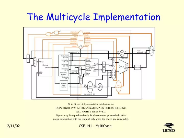
The Multicycle Implementation. Note: Some of the material in this lecture are COPYRIGHT 1998 MORGAN KAUFMANN PUBLISHERS, INC. ALL RIGHTS RESERVED. Figures may be reproduced only for classroom or personal education use in conjunction with our text and only when the above line is included.

E N D
The Multicycle Implementation Note: Some of the material in this lecture are COPYRIGHT 1998 MORGAN KAUFMANN PUBLISHERS, INC. ALL RIGHTS RESERVED. Figures may be reproduced only for classroom or personal education use in conjunction with our text and only when the above line is included. CSE 141 - MultiCycle
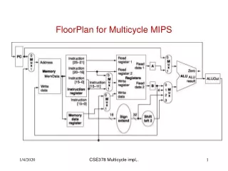
The Five Cycles • Five execution steps (some instructions use fewer) • IF: Instruction Fetch • ID: Instruction Decode (& register fetch & add PC+immed) • EX: Execute • Mem: Memory access • WB: Write-Back into registers IF ID EX Mem WB CSE 141 - MultiCycle
Summary of execution steps This is Register Transfer Language (RTL) “High level” description of changes to state elements We’ll go through these in exacting detail And translate them to “low level” control signal settings Modern design tools do this automatically CSE 141 - MultiCycle
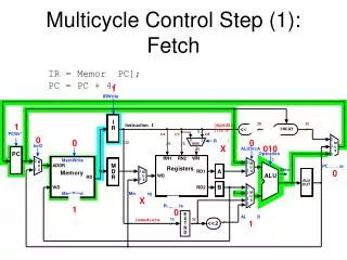
Cycle 1: Instruction Fetch Datapath: IR = Memory[PC], PC = PC + 4 (may be revised later) Control: IorD=0, MemRead=1, MemWr=0, IRwrite=1, ALUsrcA=0, etc
Control for IF cycle MemRead ALUsrcA = 0 IorD = 0 IRwrite ALUsrcB = 01 ALUop = 00 PCwrite PCsource = 00 CSE 141 - MultiCycle
Cycle 2: Instruction Decode (and register fetch) A = Reg[IR[25-21]] B = Reg[IR[20-16]] ALUout = PC + (sign-extend (IR[15-0]) << 2) We compute target address even though we don’t know if it will be used • Operation may not be branch • Even if it is, branch may not be taken Why? Everything up to this point must be instruction-independent, because we haven’t decoded the instruction. The ALU, the (incremented) PC, and the immed field are now all available CSE 141 - MultiCycle
Cycle 2: Instruction Decode cycle A = Register[IR[25-21]] B = Register[IR[20-16]] ALUout = PC + (sign-extend (IR[15-0]) << 2)
Control for first two cycles Instruction Fetch, state 0 Instruction Decode, state 1 MemRead ALUsrcA = 0 IorD = 0 IRWrite ALUsrcB = 01 ALUOp = 00 PCWrite PCSource = 00 ? Start After cycle two, we can treat different instructions separately Opcode = LW or SW Opcode = R-type Opcode = BEQ Opcode = JMP Branch Inst FSM Jump Inst FSM Memory Inst FSM R-type Inst FSM This is beginning of a Finite State Machine (FSM) specification of control. CSE 141 - MultiCycle
Cycle 3 for beq: EXecute A ALU out B In cycle 1, PC was incremented by 4 In cycle 2, ALUout was set to branch target This cycle, we conditionally reset PC: if (A==B) PC=ALUout
FSM state for cycle 3 of beq from state 1 ALUsrcA = 1 ALUsrcB = 00 ALUOp = 01 PCWriteCond PCSource = 01 To state 0 CSE 141 - MultiCycle
R-type instructions • Cycle 3 (EXecute) ALUout = A op B • Cycle 4 (WriteBack) Reg[IR[15-11]] = ALUout R-type instruction is finished CSE 141 - MultiCycle
R-type EXecution Cycle 3: ALUout = A op B Cycle 4:Reg[IR[15-11]] = ALUout A B
R-type EXecution and WriteBack Cycle 3: ALUout = A op B Cycle 4:Reg[IR[15-11]] = ALUout A ALU out B
FSM states for R-type Instructions from state 1 ALUsrcA = 1 ALUsrcB = 00 ALUop = 10 Execution ? WriteBack To state 0 CSE 141 - MultiCycle
Load and Store • EXecute (cycle 3): compute address ALUout = A + sign-extend(IR[15-0]) • Mem (cycle 4): access memory Store: Mem[ALUout] = B (store is finished) Load: MDR = Mem[ALUout] (“MDR” is Memory Data Register) • WB (cycle 5, only for load): write register Reg[IR[20-16]] = MDR Use next 5 slides to figure out control signals! CSE 141 - MultiCycle
Cycle 3 for lw and sw: Address Computation ALUout = A + sign-extend(IR[15-0])
Cycle 4 for Store: Memory Access Memory[ALUout] = B
Cycle 4 for Load: Memory Access Memory Data Register = Memory[ALUout]
Cycle 5 for load: WriteBack Reg[IR[20-16]] = memory-data
Memory Instruction states from state 1 ? Address Computation MemRead IorD = 1 MemWrite IorD = 1 Memory Access RegWrite MemtoReg = 1 RegDst = 0 To state 0 write-back CSE 141 - MultiCycle
Conditional branches and jumps • Almost all conditional branches (loops, if-then) go a short distances from the current program counter. • we can specify a relative address in many fewer bits than an absolute address • e.g., beq $1, $2, 100 => if ($1 == $2) PC = PC + 100 * 4 • But we need to be able to jump to an absolute address • jump: j 10000 means “set PC = 10000*4” • jump and link: jal 1000 means “$31 = PC + 4; PC = 1000*4” • used for procedure calls • jump register: jr $31 means “PC = $31” (used for return) CSE 141 - MultiCycle
Branch and Jump Addressing Modes • Branch (e.g., beq) uses PC-relative addressing mode (uses few bits if address typically close). That is, target is PC+displacement mode. • If opcode is 6 bits, how many bits are available for displacement? How far can you jump? • Jump uses pseudo-direct addressing mode. 26 bits of the address is in the instruction, the rest is taken from the PC. instruction program counter 6 26 4 26 00 jump destination address CSE 141 - MultiCycle
Cycle 3 for Jump PC = PC[31-28] | (IR[25-0] <<2)
Cycle 3 JMP FSM state from state 1 PCWrite PCSource = 10 To state 0 CSE 141 - MultiCycle
Control of Multicycle Implementation • We’ve been building up a Finite State Machine (FSM) • FSM shows a succession of states, transitions between states (based on inputs), and outputs for each state. • First two states are the same for every instruction, later states depend on opcode CSE 141 - MultiCycle
The complete (but fuzzy) FSM CSE 141 - MultiCycle
Simple Questions • How many cycles will it take to execute this code? lw $t2, 0($t3) lw $t3, 4($t3) beq $t2, $t3, Label #assume not taken add $t5, $t2, $t3 sw $t5, 8($t3)Label: ... • What goes on during the 8th cycle of execution? • In what cycle does the actual addition of $t2and $t3takes place? CSE 141 - MultiCycle
Implementing the FSM in hardware CSE 141 - MultiCycle
Implementing the FSM • Each state is given a number (4 bits in our design) • Datapath control signals depend only on state • Thus, control signals don’t change during ID stage • Next state may depend on opcode ... ... whenever the FSM diagram shows a choice • Last state for each opcode returns to start state • Can be implemented via random logic, PLA, or ROM. CSE 141 - MultiCycle
ROM Implementation • How many inputs bits are there? • 6 for opcode, 4 for state = 10 address lines (i.e., 210 = 1024 different addresses) • How many output bits are there? 16 datapath-control, 4 next state bits = 20 • ROM is 210 x 20 = 20K bits • Or, use a 24 x 16 for datapath, 210 x 4 for next state • Can be wasteful; for many entries, outputs are the same • in particular, opcode is often ignored CSE 141 - MultiCycle
Later, we’ll see other implementationsof the control • Microprograms are an alternate to FSM’s for specifying control signals • FSM is like a flow chart; • Microprogram is a program (written in microinstructions). • State sequencing can be done with a counter instead of an explicit “next state” function. CSE 141 - MultiCycle
Multicycle CPU Key Points • Performance can be improved by using variable-length instructions • Saves hardware but needs additional state elements • Control is more complex than single-cycle • “High level” description can be in RTL • “Low level” settings of control signals can be given by FSM (later, we’ll see microprograms) • Can implement control in combinational logic or ROM • Sequencing can use explicit “next state” function CSE 141 - MultiCycle