Download
1 / 8
90 likes | 267 Views
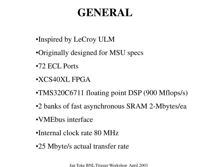
GENERAL. Inspired by LeCroy ULM Originally designed for MSU specs 72 ECL Ports XCS40XL FPGA TMS320C6711 floating point DSP (900 Mflops/s) 2 banks of fast asynchronous SRAM 2-Mbytes/ea VMEbus interface Internal clock rate 80 MHz 25 Mbyte/s actual transfer rate. Interface. FPGA.

E N D
GENERAL • Inspired by LeCroy ULM • Originally designed for MSU specs • 72 ECL Ports • XCS40XL FPGA • TMS320C6711 floating point DSP (900 Mflops/s) • 2 banks of fast asynchronous SRAM 2-Mbytes/ea • VMEbus interface • Internal clock rate 80 MHz • 25 Mbyte/s actual transfer rate Jan Toke BNL Trigger Workshop April 2003
Interface FPGA 2Mb SRAM DSP 2Mb SRAM ECL Ports Jan Toke BNL Trigger Workshop April 2003
PRESENT USES (i) MSU: Readout of TPC 16 control signals 40 data bits (5x8 bits) (ii) MSU: 32 28-bit scalers with control and readout (iii) MoNA Collaboration: Modular Neutron Array – 16 bars x 2 phototubes/module 10 modules (iv) HIRA Collaboration: Readout of the ASIC chips (LVDS adapter used) Jan Toke BNL Trigger Workshop April 2003
ECL Ports • 72 Ports configurable in quartets either as inputs,or as outputs (hardware+firmware configuration) • 4 Ports connected to dedicated clock pins of FPGA • Communicate exclusively with FPGA Jan Toke BNL Trigger Workshop April 2003
FPGA • Asynchronous (combinatorial) logic • Synchronous (registered) state machine logic • Mixed Asynchronous-synchronous logic – possible metastability • Configures via JTAG, VMEbus, or flash memory • Operations triggered via ECL ports, VMEBus, or DSP • Can interrupt VMEBus and DSP • Read/write to ASRAMS • The only internal XLM72 device communicating directly with ECL ports Jan Toke BNL Trigger Workshop April 2003
DSP • TMS320C6711by Texas Instruments • 6 ALUs running at 150 MHz = 900 Mflops/s • Boots either from ASRAM or via HPI • Triggered by FPGA, ECL ports, and VMEBus • Host Processor Interface (HPI) available for debugging and setup • Read/write from/to both banks of ASRAMs – 32 Mbyte/s • Can interrupt FPGA and VMEBus Jan Toke BNL Trigger Workshop April 2003
VMEBus Interface • 32-bit addressing mode • 32- and 16- bit data transfers • Block transfers (thus far achieved rate 25 Mbyte/s) • Read/write from/to both banks of ASRAMs • Read/write from/to FPGA • Can interrupt FPGA and DSP • Can access DSP via Host Processor Interface (HPI) Jan Toke BNL Trigger Workshop April 2003