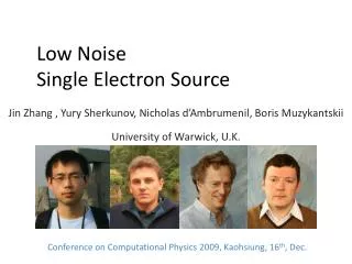
Download
1 / 20
210 likes | 543 Views
Single Electron Devices. Vishwanath Joshi Advanced Semiconductor Devices EE 698 A. Outline. Introduction Single Electron (SE) Transistor SE Turnstiles SE Pump SE Inverters Metal, Semiconductor, Carbon nano-tube SE Memory. Introduction.

E N D
Single Electron Devices Vishwanath Joshi Advanced Semiconductor Devices EE 698 A
Outline • Introduction • Single Electron (SE) Transistor • SE Turnstiles • SE Pump • SE Inverters • Metal, Semiconductor, Carbon nano-tube • SE Memory
Introduction • Devices that can control the motion of even a single electron • Consist of quantum dots with tunnel junctions • Simplest device • Single electron box
Single electron box • Conditions for observing single electron tunneling phenomena • Ec > kbT • Ec = e2/2CΣ • Rt > Rk • Rk = h/e2 (25.8 KOhms)
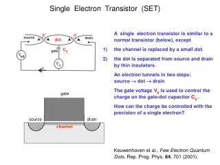
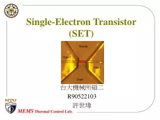
Single electron transistor • 3 terminal switching device Current flows when Vg = ne/2Cg
Turnstile • Single electron is transferred per cycle of an external RF signal • ΔEk = -e(|Q|k – Qck)/Ck • Qck = e(1+Cek/Ck)/2 • Cek = capacitance of circuit in parallel with junction k • Ck = junction capacitance Frequency Locked Turnstile Device for Single Electrons, Physical Review Letters, Vol 64(22), 28 May 1990, 2691
Pumps Accuracy of electron counting using a 7-junction electron pump, Applied Physics Letters, Vol 69 (12), 16 Sept 1996, 1804
Pumps (contd.) • Al/Al2O3 structures have limited operational temperature and poor operational stability • Si-based SETs operate at higher temperature • Place MOSFETs near SET – control of channels Electron pump by combined single-electron/field effect transistor structure, Applied Physics Letters, Vol 82 (8), 24 Feb 2003, 1221
Fabrication • Fabricated on SOI substrate using standard MOS process • Formation of Si island by PADOX method • Dual gates made of Phosphorous doped poly-Si are defined • Again deposit Phosphorous doped poly-Si and define a broad gate covering entire pattern
Measurements • Measurements at 25 K • Vth of MOSFET1 = 0.3V • Vth of MOSFET2 =-0.2V
Charge Coupled Device • 30 nm wide Si-wire channel and poly-Si gates defined by E-beam lithography Current quantization due to single electron transfer in Si-wire charge coupled device, Applied Physics Letters, Vol 84 (8), 23 Feb 2004, 1323
Si SE Inverter • Twin Si single electron islands are formed by V-PADOX Si complementary single-electron inverter with voltage gain, Applied Physics Letters, Vol 76 (21), 22 May 2000, 3121
SE Inverter (contd.) • Working of Inverter
Al/Al2O3 SE Inverter • 25 nm thick Al patterned to form the lower electrodes • Al oxidized in an O2 plasma, 200 mTorr, 5 min, 200 oC • Second Al deposition Single-electron inverter, Applied Physics Letters, Vol 78 (5), 19 Feb 2001, 1140
Al/Al2O3 SE Inverter (contd.) • Working of Inverter
SE Inverter from carbon nanotubes • Tunnel barriers fabricated with the local irradiation of an Ar beam Fabrication of single-electron inverter in multiwall carbon nanotubes, Applied Physics Letters, Vol 82 (19), 12 May 2003, 3307
SE Inverter from carbon nanotubes (contd.) • Working of the Inverter
References • Frequency Locked Turnstile Device for Single Electrons, Physical Review Letters, Vol 64(22), 28 May 1990, 2691 • Accuracy of electron counting using a 7-junction electron pump, Applied Physics Letters, Vol 69 (12), 16 Sept 1996, 1804 • Electron pump by combined single-electron/field effect transistor structure, Applied Physics Letters, Vol 82 (8), 24 Feb 2003, 1221 • Current quantization due to single electron transfer in Si-wire charge coupled device, Applied Physics Letters, Vol 84 (8), 23 Feb 2004, 1323 • Si complementary single-electron inverter with voltage gain, Applied Physics Letters, Vol 76 (21), 22 May 2000, 3121 • Single-electron inverter, Applied Physics Letters, Vol 78 (5), 19 Feb 2001, 1140 • Fabrication of single-electron inverter in multiwall carbon nanotubes, Applied Physics Letters, Vol 82 (19), 12 May 2003, 3307 • A high-speed silicon single-electron random access memory, IEEE Electron Device Letters, Vol. 20, No. 11, November 1999, 583