Download
1 / 10
100 likes | 263 Views
FPGAs for high performance – high density applications. Intro Requirements of future trigger systems Features of recent FPGA families. 9U * 40cm. ATCA. µ TCA/AMC. Intro : FPGA basics. Large array of logic cells ~100k

E N D
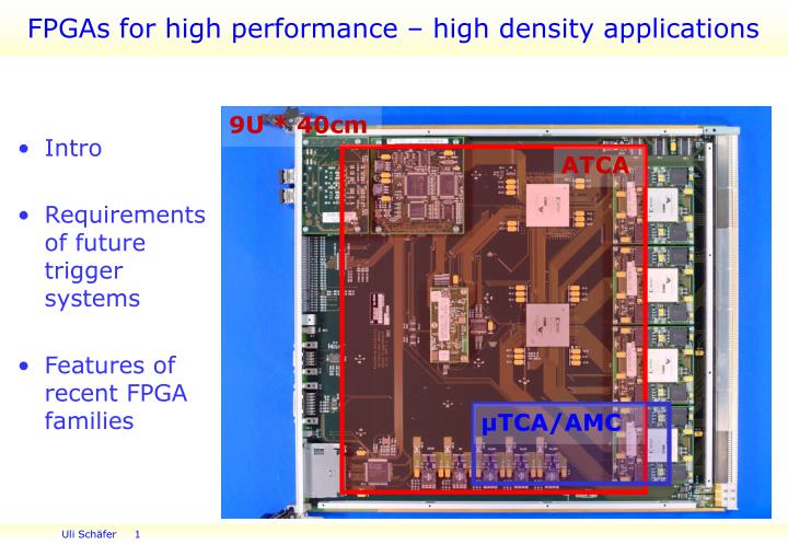
FPGAs for high performance – high density applications • Intro • Requirements of future trigger systems • Features of recent FPGA families 9U * 40cm ATCA µTCA/AMC
Intro : FPGA basics • Large array of logic cells ~100k • combinatorial : map any 4-variable equation into 4-input lookup table (LUT) • sequential : flip-flop (FF) • Interconnect • ‘wires’ : segmented routing • switch boxes connecting wires and logic cells • dedicated global clock trees into all cells • I/O pads • route internal signals to pins • define signal standard • Clock management : condition the incoming clocks and generate multiples and fractions • phase lock loop (PLL) • delay lock loop (DLL) • Cores • RAM blocks for data storage • Many other cores introduced in recent years, see below… • Functionality of FPGA is defined upon power up by reading in a configuration data stream from non-volatile memory
Requirements of future L1calo processors • Higher granularity along with the need to keep fraction of duplicated channels at reasonable level requires higher density designs (higher channel count per FPGA and per module) • Typical form factors and therefore card edges tend to get smaller: • current L1calo ‘standard’ is 9U*400mm • Telecom standards : ATCA: 8U * 280mm µTCA (AMC): 73.5 * 180.6mm • Narrower data paths, but 10/12.5 Gbps per link • Single ended data transmission stretched to limits at data rates and signal standards employed on current L1calo modules go differential FPGA features in demand: • on-chip high-speed serial links ( incoming trigger tower data ) • differential high-speed data buses ( FIO ) • logic resources (fabric) • arithmetic units in case more demanding algorithms required • suitable pinout and I/O properties for high density / high speed designs (signal integrity)
Recent FPGA features/improvements • Increase in clock speed • Increase in logic resources (fabric) • Increase in block memory • Further hard cores: • Processors • Gbps serializer/deserializer units for parallel source synchronous data transmission (clock forwarding) • Multi-Gbps links with embedded clock • DSP / arithmetic circuitry • I/O • Differential high-speed standards (LVDS,PECL,…) • Low voltage single ended • Internal termination • differential : 100Ω • single ended : ‘programmable’ impedance • On-chip bypass capacitors and signal integrity-optimised pinout
Resources by manufacturer (*) All FPGA families have some means of phase adjustment (L,X) or multi-phase sampling (A) on their input lines, as well as SerDes. Not all features available on all I/O linesVirtex-4 have 6.5 Gbps serial links
Lattice SC input delay control • 144 tap delay unit, 40ps/tap • 9-tap sampling within a window allows for calculation of optimum sampling point and automatic delay adjustment • Available on every other differential pair only
Xilinx Virtex-5 source synchronous interface (Gbps, double data rate) • SerDes and programmable delay unit available in all I/O pads • No hard core phase aligner, use soft core (fabric) to track data • Eliminate cycle-to-cycle jitter at source with a PLL • Due to the DLL the data are clocked into the deserialiser with a clock edge generated just a few ticks before the data bit Low frequency jitter doesn’t matter
Xilinx serial links (MGT) • 3.7 Gbps serial link, low power 100mW/ch • up to 24 channels per device Data rate and channel count match SNAP12 optical link • Transmitter: programmable signal level pre-emphasis • Receiver: equalization • Latency (RX+TX) : minimum of 12.5 ticks of byte clock • byte clock could be as high as 320 MHz for a 40 MHz based system • 40ps reference clock jitter requirement • Re-design LHC clock distribution • Use jitter attenuators (silabs.com) • Go asynchronous • Use local Xtal • Require re-synchronisation to LHC clock (latency !) • Allow for standard data rates / standard components
Xilinx Virtex-5 resources (maximum) Resource Virtex-5 (in XCV1000E) 6-input LUTs: 200k (25k*4-input) Flipflops: 200k (25k) Distributed RAM : 3.4 Mb (400kb) Block RAM : 11.6Mb (400kb) “DSP” 25*18 bit multiplier/accumulator: 640 PCI Express endpoint 1 Ethernet MAC (with internal or external PHY) 4
Summary / Outlook • Logic density gone up considerably. A single FPGA is equivalent to almost a full L1calo processor module • Current FPGA families allow for high data rates on both ‘parallel’ and high-speed serial links • Aggregate bandwidth is higher on ‘parallel’ links • Xilinx Virtex-5 has same high-speed I/O resources on all user pins and is therefore particularly useful for typical trigger circuitry : many-in few-out • On-chip links with embedded clock do have surprisingly low latency but might need additional synchroniser stages due to jitter requirements Xilinx development boards ML506/ML555 available let’s start work. Explore synchronous / asynchronous schemes