Download
1 / 11
110 likes | 398 Views
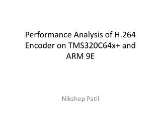
TMS320C64X 框图. TMS320DM642 的主要特性. 500MHz core at 1.2V; 600MHz core at 1.4V Memory Architecture 16K L1D, 16K L1P, 256K L2 64-channel Enhanced DMA 133 Mhz, 64-bit EMIF 3 Video Ports Each configurable for Capture or Display Dual 8/10-bit BT656 or raw modes

E N D
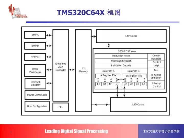
TMS320DM642的主要特性 500MHz core at 1.2V; 600MHz core at 1.4V Memory Architecture • 16K L1D, 16K L1P, 256K L2 64-channel Enhanced DMA 133 Mhz, 64-bit EMIF 3 Video Ports • Each configurable for Capture or Display • Dual 8/10-bit BT656 or raw modes • 16/20-bit raw modes and 20-bit Y/C for high definition • Horz Scaling and Chroma Resampling Support for 8-bit modes • Supports Transport Interface mode 10/100 Ethernet MAC (muxed w/ PCI) Serial Ports • McASP (Multi-channel Audio Serial Port) • McBSP • IIC 3 32-bit Timers Additional 16-bit GPIO Host/backplane Connection Either • 66 MHz PCI • HPI32 • HPI16 and Ethernet MAC
DM642 Processor EMIF 64 VCXO InterpolatedControl (VIC) Power Down PLL PCI-66 or HPI32 L1P Cache 16 KBytes or HPI16 and EMAC/MDIO C64xTM DSP Core Instruction Fetch Control Registers Interrupt Control Instruction Dispatch 20-bit Video Port 0 (VP0) 10-bit VP0 In-Circuit Emulation Instruction Decode and or or 2 10-bit VP0 Data Path 1 Data Path 2 McBSP0 or McASP Enhanced DMA Controller A Register File B Register File L2 Cache/Memory 256 KBytes L1 S1 M1 D1 D2 M2 S2 L2 20-bit Video Port 1 (VP1) 10-bit VP1 and or or 2 10-bit VP1 L1D Cache 16 KBytes McBSP1 or McASP Timer 0 Timer 1 20-bit Video Port 2 (VP2) Timer 2 Or 2 10-bit VP2 GPIO16 IIC0 TMS320DM642框图
多核系统(以OMAP5910 处理器为例) DSP器件从传统的通用型处理器中分离出更多的直接 面向特定应用对象的SoC。 如DSP+ARM的双核SoC器件。 以TI公司为例: OMAP1510:面向第3代无线通信终端 (为了开辟手机芯片市场,TI专门成立了平行于DSP组的 无线芯片组,下设OMAP分部,专门为手机开发处理器); DM270:面向数码相机; DA610:面向专业音频设备; DM642:面向媒体处理。
TI的ARM+DSP结构产品线 数字音频处理: DSP54x+ARM7+Ethernet MAC 数字视频处理:DSP54x+ARM7(9)+IMX 多媒体通信: DSP55x+ARM9 高性能视频处理:DSP64x+ARM
ARM与DSP数据处理机制 OMAP 5910 产品 Real-Time Processing DSP OS / Control RISC The Right Part for the Right Task DSP RISC • 操作系统 • 控制、用户界面 • 通信 • 多媒体处理
ARM与DSP数据处理机制 OEM 应用 Open Source Software Third Party Software 应用 3rd Party Apps Java Apps JVM Applications Technology Open SourceApplications Java VM TI Technology Run-time Library (GNU libc or uClibc) GStreamer OEM Algorithms Linux 内核 Scheduler, file system, networking stack DSPLinux Bridge DSP Algorithms Code Compression Power Management BIOS II Board Specific Software Boot Loader Frame Driver Network Drivers Bridge Driver DSP Hardware (C54xTM, C55xTM, C6xTM DSPs etc.) Hardware RISC Hardware (ARM7,ARM9)
TI OMAP5910的结构特点 • 双核结构( ARM925T + DSP55x ) • 基于ARM9TDMI的微控制器单元 16K-byte指令缓存和8K-byte数据缓存 存储器管理单元 (MMUs) 17-word 写缓冲单元 • DSP55x 数字信号处理单元 48K-word SARAM 32K-word DARAM 16K-word ROM 24K-byte 指令缓存
TI OMAP5910的结构特点 • 一个交通控制器,用于集中控制处理器的内存访问和输入输出 • 一个ARM端9通道系统DMA控制器和一个LCD专用通道 • 一个DSP端6通道DMA控制器 • DSP的存储器管理单元(MMU) • 3个DSP端硬件加速器(for DCT,iDCT,像素内插和运动估计) • MPU接口(MPUI) • 本地总线接口(with MMU)
TI OMAP5910的结构特点 • DSP 私有外设 (只能由 DSP访问)3个定时器、1个看门狗、 Level 1/Level 2 中断管理器 • DSP 公共外设(由 DSP, DSP DMA和MPU通过MPUI访问) 2个多通道缓冲串口(McBSPs)、 2个多通道串行接口 (MCSIs) • MPU 私有外设 (只能由MPU访问) 3个定时器、1个看门狗、Level 1/Level 2中断管理器、LCD 控制器
TI OMAP5910的结构特点 • MPU 公共外设 (由 MPU和系统DMA访问) 多通道缓冲串口(McBSP) I2C 主从接口 照相机接口 键盘接口 MMC/SD接口(也可配置为通用SPI口) • MPU/DSP 共享外设 (MPU选择由哪个处理器来控制) 4个Mailboxes用于内部处理器通信 14个通用I/O(GPIOs) 3个UARTs