Download
1 / 1
10 likes | 168 Views
3D TRANSISTORS Matt Goranson, Oklahoma State University ECEN 5843 Spring 2014. Introduction. Benefits, cont. Applications.

E N D
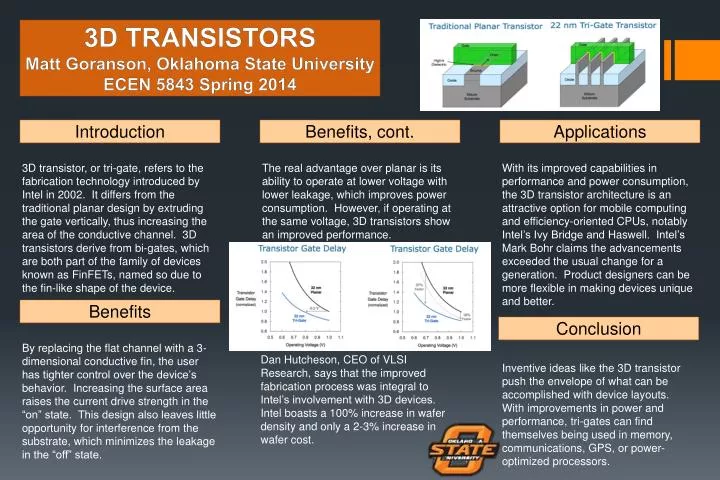
3D TRANSISTORS Matt Goranson, Oklahoma State University ECEN 5843 Spring 2014 Introduction Benefits, cont. Applications 3D transistor, or tri-gate, refers to the fabrication technology introduced by Intel in 2002. It differs from the traditional planar design by extruding the gate vertically, thus increasing the area of the conductive channel. 3D transistors derive from bi-gates, which are both part of the family of devices known as FinFETs, named so due to the fin-like shape of the device. The real advantage over planar is its ability to operate at lower voltage with lower leakage, which improves power consumption. However, if operating at the same voltage, 3D transistors show an improved performance. With its improved capabilities in performance and power consumption, the 3D transistor architecture is an attractive option for mobile computing and efficiency-oriented CPUs, notably Intel’s Ivy Bridge and Haswell. Intel’s Mark Bohr claims the advancements exceeded the usual change for a generation. Product designers can be more flexible in making devices unique and better. Benefits Conclusion By replacing the flat channel with a 3-dimensional conductive fin, the user has tighter control over the device’s behavior. Increasing the surface area raises the current drive strength in the “on” state. This design also leaves little opportunity for interference from the substrate, which minimizes the leakage in the “off” state. Dan Hutcheson, CEO of VLSI Research, says that the improved fabrication process was integral to Intel’s involvement with 3D devices. Intel boasts a 100% increase in wafer density and only a 2-3% increase in wafer cost. Inventive ideas like the 3D transistor push the envelope of what can be accomplished with device layouts. With improvements in power and performance, tri-gates can find themselves being used in memory, communications, GPS, or power-optimized processors.