Download
1 / 35
350 likes | 459 Views
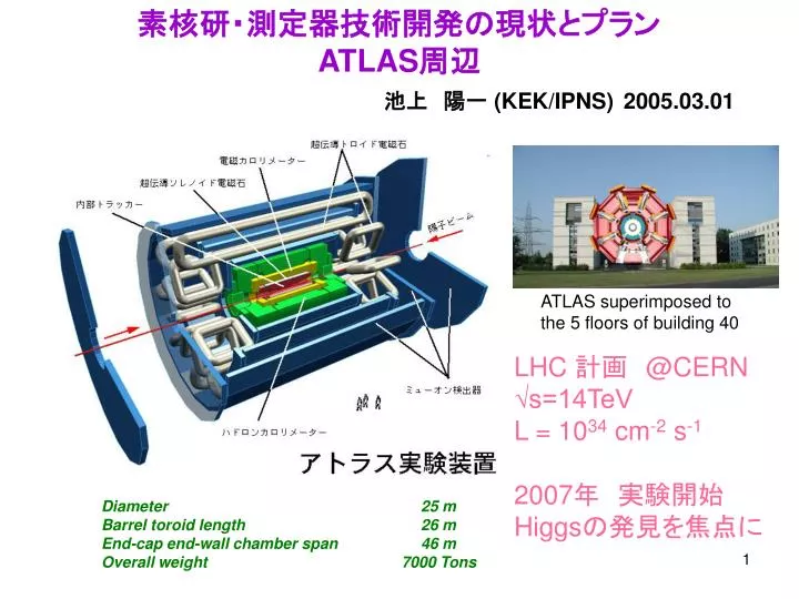
素核研・測定器技術開発の現状とプラン ATLAS 周辺 池上 陽一 (KEK/IPNS) 2005.03.01. ATLAS superimposed to the 5 floors of building 40. LHC 計画 @CERN √s=14TeV L = 10 34 cm -2 s -1 2007 年 実験開始 Higgs の発見を焦点に. Diameter 25 m Barrel toroid length 26 m End-cap end-wall chamber span 46 m

E N D
素核研・測定器技術開発の現状とプランATLAS周辺池上 陽一 (KEK/IPNS) 2005.03.01 ATLAS superimposed to the 5 floors of building 40 LHC 計画 @CERN √s=14TeV L = 1034 cm-2 s-1 2007年 実験開始 Higgsの発見を焦点に Diameter 25 m Barrel toroid length 26 m End-cap end-wall chamber span 46 m Overall weight 7000 Tons
アトラス国際チームの財政分担・参加機関・研究者数(トップ10)アトラス国際チームの財政分担・参加機関・研究者数(トップ10)
ATLAS 測定器の構成(赤は日本グループが関与) • Magnets -- Central Superconducting Solenoid (B=2T) -- Barrel and Endcap Superconducting Toroids (Bdl=2~8Tm) • Tracking (||<2.5): -- Silicon pixels detector -- Silicon microstrip detector -- Transition radiation detector • Calorimetry (||<5): -- EM : Pb-LAr -- HADRON: Fe/scintillator (central), Cu-LAr (endcap) -- Forward : Cu-LAr(EM) + W-LAr (hadron) • Muon Spectrometer (||<2.7) : -- Precision chambers : MDT, CSC(fwd) -- Trigger system : RPC(barrel), TGC(endcap)
Barrel Silicon microstrip detector(SCT : Semiconductor Tracker ) ×2,112 modules → Total area = 34m2 radiation tolerance 3×10¹⁴ n/cm2 (10 years) 4 cylinders r = 30~52cm |η|<1.4 First complete barrel cylinder at Oxford U. December 2004 ↓ CERN
Barrel SCT modules Specifications: Strip pitch : 80 μm Stereo angle : 40 mr readout channels ; 1536 ch ~ 5000 wire bondings Assembly accuracy < 5 μm Parts: 4 Silicon sensors (Hamamatsu) 12 ABCD chips (BiCMOS ASIC) TPG thermal conductor (UK) Flexible hybrid circuit (Japan) Fablication: Total: 2600 modules 980 in Japan (best yield > 95%) Others in UK, US and Scandinavia
module-mounting robots Two module-mounting robots designed and supplied by KEK.
Barrel SCT における主要な測定器技術開発 • Radiation-hard Si センサーの設計開発 • High-density low-mass Readout Hybrid(COB)の設計開発 • 1μm精度のmoduleの組み立て、及び検査方法の確立 • 5K wire bondings x 1K module -> 5M WBsの経験 • module-mounting robot の設計開発 • Laser による Module検査方法の確立 • IRカメラによるSi センサーの不良解析
アトラス超伝導ソレノイド:KEKが提案・設計・開発・建設を100%担当アトラス超伝導ソレノイド:KEKが提案・設計・開発・建設を100%担当 ・電磁カロリメターの内側なので肉厚を極力薄くした: → 高強度のアルミニウムを採用(古河・日立電線と技術開発) → クライオスタットを液体アルゴンカロリメータと共用
アトラス超伝導ソレノイド (日本が担当) 東芝京浜工場(1999年) 励磁成功(2000年12月) CERNに到着(2001年9月) Maiani所長らと LArクライオスタットへ据付(2004年2月)
2004年7月5日:CERN地上試験で8197アンペアを達成した。通常の運転電流は7600アンペアである。2004年7月5日:CERN地上試験で8197アンペアを達成した。通常の運転電流は7600アンペアである。 2004年10月にアトラス地下実験場に運搬された。
TGC • Thin Gap Chambers (TGCs) are used for the muon trigger system in the end-cap regions of the ATLAS detector at Large Hadron Collider(LHC). Muon spectrometer (air-core Toroid) Toroid Magnets Hadron Calorimeter 22m • TGC at ATLAS detector • Total 3600 chambers • 320,000 read-out channels • Total area ~2,000m2 43m Solenoid Magnet Inner Detector EM Calorimeter
1.3m 1.4m Thin Gap Chamber Requirements on ATLAS: • Fast signal response (<25ns) • High efficiency (>98 %) • Radiation-proof (~0.6C/cm) • Rate capability (~kHz/cm2) ASD: Amp. Shaper Discriminator
1998 1999 2000 2001 2002 2003 2004 Test production T7 type production 672 chambers T4 192 T5 192 Checking quality Graphite spraying 80 boards/month 4 board /day Mounting Read-out boards 1 Unit/day 3 persons FR4 Frame Gluing Wire winding 2 boards /day 1 person 4 boards/day 3 persons Making doublet (triplet) Singlet closing 1 Unit/day 2persons 2 TGCs /day 3 persons Paper honeycomb
TGC chamber Quality Control • TGC is fabricated by the gluing processes (we can no longer reopen it after closing TGC). • We have to control the surface distortion less than 200 mm • We apply following tests: • Measurement of the surface resistance of cathode after the graphite spraying, • High voltage test before and after closing singlet TGC, • Pulse test after mounting adapter board and • High voltage test after mounting adapter board. • Pulse response check by b-ray radioactive source • Cosmic ray test at KOBE Univ.
Graphite spraying and FR4 frame Gluing • Graphite spraying by automatic sprayer • two-dimensional linear actuator • spray gun by the pneumatic control AT FR4 Frame gluing : To control the quality of epoxy adhesive. Screen painting method for parts and Auto dispenserfor button supports are adopted.
Wire winding Anode Wire: Gold plated Tungsten (A.L.M.T. co. Ltd.) Solder: Sn(80)+Zn(20) Flux: Water soluble flux (including: ZnCl2+ZnNH4) Wire winding machine • Consists of a linear actuator and a rotating table. Total ~800,000 wires for all TGCs
TGC closing • In order to make flat plane, the combination of the vacuum-press and the suction plate technique have been adapted. Number of measured points
Making doublet modules • In order to make TGC flat, • Aluminum honeycomb keeps upper TGC. • Granite table keeps lower TGC by –40 kPa pressure. • The gas volume of the singlets TGC is slightly over-pressured (150 pa) as counter force against the force on the rubber sheet. TGC
Detector performance Bad sample • Cosmic ray test at KOBE Univ. • Position dependence of the efficiency was measured with a granularity of 5mm-by-5mm.
TGC chamber Summary • 1200 TGCs have been produced in Japan • We created the required environment to make 2 TGCs/day. • We have to make uniform quality • Controlling the TGC’s surface distortion <200 mm • We have developed some tools (screen painting method or air control at gluing)
Atlas TGC ASICs • 320k channels Muon Trigger Chambers • L1 Trigger and Readout Circuits • Synchronous (40MHz) track finding circuits (<20 clks latency) • 100 kHz trigger rate • On-detector electronics • 耐放射線性 (全ての半導体の照射試験を行う) • TID:50 krad (最大時:安全係数込み) • SEE:2.11x10¹⁰ h/cm2/10 years (安全係数なし) • FPGAが使用出来ない • 許容消費電力、スペースの制限 • チャンネル単価 : 目標 \1,000/ch (全エレキシステムで) • 4種類のASICの開発 • Atlas TGC日本グループとKEK回路室 • ASD, Patch-Panel ASIC, SLB ASIC, H-pT ASIC
Amplifier-Shaper-Discriminator (ASD) • SONY Bipolar Analog Master Slice • 回路設計全てを自前で行い、配線レイアウト、プロセスのみをソニーに委託 • 4-ch per chip • 量産 • 100k chips for Atlas • 10k chips for PS Exp. • 積分時間変更版 • 京大(谷森研)-KEK • 23k chips共同購入 • J-PARC等からの要請 • Higher gain from MPGC (JAERI) • New process
Patch-Panel ASIC and SLB ASICVDEC-Rohm full-custom 0.35mm CMOS • 回路設計、レイアウト設計全て自前 • アナログ回路の設計 • LVDS Rx • Variable Delay (sub-ns step, PLL control) • Test Pulse Generator • 初段trigger matrix回路、読み出し回路 • JTAG Control • 量産 • PP ASIC(5mm角) 25k 済み • SLB ASIC(10mm角) 5k • 度重なる失敗を繰り返し、ついに完成 4月量産予定
H-pT ASICVDEC-Hitachi 0.35mm CMOS Gate Array • 回路設計、レイアウト設計全て自前 • 第2段trigger matrix (all logic) • FPGA感覚で出来た! • でも、後からバグが見つかったりする。外付け回路で逃げる。 • 1.2k chips 量産 • FPGAでは無理? • 放射線SEE • 多入出力 • 多配線資源 • 多Flip-Flop • FPGA自動配置 配線では辛い
ATLAS Muon TDC (AMT) chip • ミューオン検出器用TDC ~40万チャンネル • 400 kHz/ch最大入力レート, 100 kHz トリガーレート • 立ち上がり/下がり(幅)エッジ時間測定 • 781 ps/bit, 250 ps RMS 分解能 • トリガーに対応したデータのみ選択出力 • 80 Mbps Serial/32bit Parallel Output • 放射線耐性 ( >50 krad, Low SEE, > 10year LHC) • Double Hit Resolution ~5 ns • 安価(¥200/ch), 低電力 (~15 mW/ch) & 高密度 (24 ch/chip) • 0.3 m CMOS
ASD AMT ATLAS MDT Front-end Electronics 信号の立ち上がり/下がり及びスルーレートの測定を行う。
ATLAS AMT 現状 • 20,000チップ量産終了。 • 17,000 Frontend Board生産終了。 • 現在チェンバーへの取付中。 他実験での応用 • AMT-VME ボード(~100台販売), K2K, Cangaroo,理研… • Bellアップグレード(Copper TDC Finessボード) • Bepi Colimbo水星探査衛星(宇宙科学研)搭載予定。 • Super-Kアップグレード(〜4万チャンネル)使用予定。 • Ionwerks Inc.微量分析装置(米国)
次期測定器技術開発のプラン • LHC upgrade (SuperLHC)のシナリオ • 実験開始 • Low luminosity run • 2010 High luminosity run Higgs (or SUSY)発見か • 発見から精密測定のphaseへ • 2014 focusing quadrupole の radiation limit < 700 fb-1 • upgradeの可能性を検討 • luminosity × 10 (1034 → 1035 cm-2s-1) √s × 2 • ATLAS全体としてもUpgradeの詳細な検討が開始 • Workshop on ATLAS Upgrades for High Luminosity (2005.02) R&D 開始 (3年) 量産開始 (5年) install
Detector upgrades for SLHC Magnets Calorimeter Muon Spectrometer OK (need minor changes) Inner Tracker Need major detector upgrades due to radiation damage and large occupancy pixels detector 6×10¹⁵ n/cm2 Si microstrip detector3×1014 n/cm2 Transition radiation detector 6×10¹³ n/cm2 (chamber) 10years × 10 Radiation damege → charge collection の悪化、 S/Nの悪化 leakage current の増大、 full depletion voltage の増大 coolingの負担 (-10℃) HV PSの負担
SCT upgrades R&D strip type short strip stripixel channel数を押さえる工夫 long pixel Wafer : radiation hard Si sensor n- type bulk(radiation damege を受けて p- にtype inversion) → p- type bulk (waferの安定な入手が困難) Standard Floating Zone (高抵抗単結晶Siの製法の標準) Diffusion oxygenated FZ Czochralski oxygen rich → rad hard Magnetic Cz Epitaxial layers on Cz-substrates n- type bulk は使えないのか? n- strip (w/ p- stop) in n- bulk Thin layer 量産可能な技術であること
SCT upgrades R&D (2) Readout ASIC Deep sub-micron CMOS Technology CERN successfully developed rad-hard DSM technology (IBM 0.25 μm) SiGe BICMOS Technology Low power, High speed, Low noise (radiation hard?) Irradiation test facility 3×10¹⁵ n/cm2 Irradiation test が必要。 KEK PS EP1A (2×10¹² PPP) →1week 放射化物質の移動 → 国内で、行いたい
AMTブロック図 Chamber Resolution
Summary • 1200 TGCs have been produced in Japan • We created the required environment to make 2 TGCs/day. • We have to make uniform quality • Controlling the TGC’s surface distortion <200 mm • We have developed some tools (screen painting method or air control at gluing)