Download
1 / 68
1.1k likes | 1.89k Views
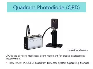
Noise In Photodiode Applications. By Art Kay and Bryan Zhao ( 赵 伟 ) June 1, 2011. Noise Review Photodiode Review Photodiode Noise Theory Bandwidth and Stability OPA827 Hand Calculation OPA827 Tina Spice Analysis OPA827 Measurement Example. Contents. Noise Review. Intrinsic Noise

E N D
Noise In Photodiode Applications By Art Kay and Bryan Zhao ( 赵 伟 ) June 1, 2011
Noise Review Photodiode Review Photodiode Noise Theory Bandwidth and Stability OPA827 Hand Calculation OPA827 Tina Spice Analysis OPA827 Measurement Example Contents
Noise Review
Intrinsic Noise • Error Source • Generated by circuit itself (not pickup) • Calculate, Simulate, and Measure
Time Domain – White noise normal distribution
Noise is a key parameter in photodiode design Wide bandwidth (integrate more noise) Low signal levels (noise more critical) Photodiode amplifier noise is more complex Parasitic capacitance and sensor capacitance Poles and zeros Gain peaking Why Photodiode Noise?
What can we do with the photodiode knowledge? The competition is in trouble! Our new friends from National. TI
Photodiode Review
Photodiode Basics • Introduction • Photodiodes convert light into current or voltage. • Photodiode type • PN photodiode – more wavelength selective • PIN photodiode – wide spectral range (less selective) • APD (Avalanche photodiode) – sensitive to low light, fast
Figure1.3 Photodiode Equivalent Circuit Figure1.4 Current VS. Voltage Characteristics Photodiode Basics
Figure1.4 Photodiode Equivalent Circuit Figure1.5 Current VS. Voltage Characteristics Photodiode Basic Use left equivalent circuit, the output current is given as : The open circuit voltage Voc is the output voltage when Io equals 0. Thus Voc becomes:
Photodiode and Control Source TINA model Light exciting source: 1) Use VG1 and VG2 voltage sources to simulate light power wave. 2) Use R1 and C1 shape light signal 3) The Voltage Control Current Source (VCCS1) simulates photodiode sensitivity. Photodiode Equivalent Circuit: 1), Current Source Id simulates Dark current 2), Diode is a ideal diode 3), Cd and Rd simulate photodiode's junction capacitor and dark Resistance. 4), Rs is series resistor, which is far smaller than Rd.
Photodiode Noise Theory
Noise Gain Simplify the model to compute Noise Gain Gain seen by the noise voltage source.
Simulating Noise gain and noise bandwidth • Break the loop to measure Aol, 1/B, and I to V Gain
Voltage Noise eni , eno and Eno Region 1 Region 2 Region 3 Region 4 Region 5 Eno4 Eno5 Eno3 Eno1 Eno2
Voltage Noise eni , eno and Eno Region 1 noise: Region 2 noise: Region 3 noise: Region 4 noise: Region 5 noise: Total voltage noise:
Voltage Noise eni , eno and Eno eno Log scale R.1 R.4 R.2 R.3 R.5 Eno^2 Linear scale eno Linear scale
Resistor Noise and Current Noise Current noise and resistor noise are limited by the transimpedance (I-V gain) bandwidth
Bandwidth and Stability
Parasitic Capacitance Limits the Bandwidth • Max bandwidth with Min Cf • Low Cf may be unstable • Wide BW increases noise • As shown Cf=Cs (stray cap)
Feedback Capacitance Required for Stability • Noise Gain is key to stability • Also called 1/Beta (in stability analysis) • ROC = Rate of Closure • ROC = (Aol slope) – (1/Beta slope) • Unstable when ROC > 20dB/decade
Feedback Capacitance Required for Stability Applying a Step Input shows instability at output
OPA827 Hand Calculation
Example Photodiode: PDB-C158 Unfortunately Cj is not specified at Vr=0V. We called the manufacturer for this info Cj=70pF for Vr=0V
Advantage Reduces noise to zero Available on E-Bay Disadvantage Requires 1.21 gigawatts Size Flux Capacitor ADS1118 Quarter
OPA827 Tina Spice Analysis
OPA827 – test the model • Low Noise : 4nV/√Hz at 1kHz • Low Offset Voltage: 150µV max • JFET Input: IB= 15pA typ • Wide Bandwidth: 22MHz The noise performance is the same as datasheet.
Simulated Spectral Density and Total Noise Output Noise Density Total Output Noise
OPA827 Measurement Example