Download
1 / 62
620 likes | 639 Views
Explore the fundamentals of memory systems in Computer Science, including Register Files within the CPU, Tri-state devices for Scaling Memory, SRAM Cache, and DRAM Memory. Learn how to store and access data efficiently in processors.

E N D
Memory Prof. Hakim Weatherspoon CS 3410 Computer Science Cornell University [Weatherspoon, Bala, Bracy, and Sirer]
Announcements Make sure you are • Registered for class, can access CMS • Have a Section you can go to. • Lab Sections are required. • “Make up” lab sections only Friday 11:40am or 1:25pm • Bring laptop to Labs • Project partners are required for projects starting w/ project 2 • Project partners will be assigned (from the same lab section, if possible)
Announcements • Make sure to go to yourLab Section this week • Completed Proj1 due Friday, Feb 15th • Note, a Design Document is due when you submit Proj1 final circuit • Work alone BUT use your resources • Lab Section, Piazza.com, Office Hours • Class notes, book, Sections, CSUGLab
Announcements Check online syllabus/schedule • http://www.cs.cornell.edu/Courses/CS3410/2019sp/schedule • Slides and Reading for lectures • Office Hours • Pictures of all TAs • Project and Reading Assignments • Dates to keep in Mind • Prelims: Tue Mar 5th and ThurMay 2nd • Proj1: Due next Friday, Feb 15th • Proj3: Due before Spring break • Final Project: May 16th Schedule is subject to change
Announcements • Level Up (optional enrichment) • Teaches CS students tools and skills needed in their coursework as well as their career, such as Git, Bash Programming, study strategies, ethics in CS, and even applying to graduate school. • Thursdays at 7-8pm in 310 Gates Hall, starting this week • http://www.cs.cornell.edu/courses/cs3110/2019sp/levelup/
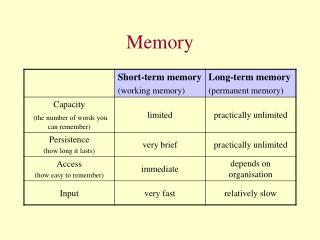
Goals for today Memory • CPU: Register Files (i.e. Memory w/in the CPU) • Scaling Memory: Tri-state devices • Cache: SRAM (Static RAM—random access memory) • Memory: DRAM (Dynamic RAM)
Last time: How do we store one bit D Q D Flip Flop stores 1 bit clk
Goal for today How do we store results from ALU computations?
Big Picture: Building a Processor memory registerfile inst alu +4 +4 addr =? PC din dout control cmp offset memory new pc target imm extend A Single cycle processor
Big Picture: Building a Processor memory registerfile inst alu +4 +4 addr =? PC din dout control cmp offset memory new pc target imm extend A Single cycle processor
Goal for today How do we store results from ALU computations? How do we use stored results in subsequent operations? Register File How does a Register File work? How do we design it?
Register File Register File • N read/write registers • Indexed by register number Dual-Read-PortSingle-Write-Port 32 x 32 Register File QA 32 DW 32 QB 32 W RW RA RB 1 5 5 5
Register File D0 Recall: Register • D flip-flops in parallel • shared clock • extra clocked inputs:write_enable, reset, … D1 D2 D3 4-bit reg 4 4 clk clk
Register File D0 Recall: Register • D flip-flops in parallel • shared clock • extra clocked inputs:write_enable, reset, … D1 D2 D3 32-bit reg 32 32 clk clk
Register File 32 D …. Register File • N read/write registers • Indexed by register number How to write to one register in the register file? • Need a decoder Reg 0 Reg 1 Reg31 Reg30 5-to-32 decoder addix1, x0, 10 5 RW W 00001
Aside: 3-to-8 decoder truth table & circuit 3-to-8 decoder … 001 3 RW
Aside: 3-to-8 decoder truth table & circuit 3-to-8 decoder … 001 3 RW i2 i1 i0 o0 i2 i1 i0 o5
Register File 32 …. Register File • N read/write registers • Indexed by register number How to read from two registers? • Need a multiplexor Reg 0 32 M U X Reg 1 …. QA Reg30 Reg31 add x1, x0, x5 M U X 32 …. QB 5 5 RA RB
Register File 32 D 32 …. Register File • N read/write registers • Indexed by register number Implementation: • D flip flops to store bits • Decoder for each write port • Mux for each read port Reg30 Reg31 Reg 0 Reg 1 32 M U X …. QA 5-to-32 decoder M U X 32 …. QB 5 5 5 RA W RW RB
Register File Register File • N read/write registers • Indexed by register number Implementation: • D flip flops to store bits • Decoder for each write port • Mux for each read port Dual-Read-PortSingle-Write-Port 32 x 32 Register File QA 32 DW 32 QB 32 W RW RA RB 1 5 5 5
Register File What happens if same register read and written during same clock cycle? Register File • N read/write registers • Indexed by register number Implementation: • D flip flops to store bits • Decoder for each write port • Mux for each read port
Tradeoffs 8-to-1 mux a Register File tradeoffs + Very fast (a few gate delays for both read and write) + Adding extra ports is straightforward – Doesn’t scale e.g. 32Mb register file with 32 bit registers Need 32x 1M-to-1 multiplexor and 32x 20-to-1M decoder How many logic gates/transistors? b c d e f g h s2 s1 s0
Takeway Register files are very fast storage (only a few gate delays), but does not scale to large memory sizes.
Goals for today Memory • CPU: Register Files (i.e. Memory w/in the CPU) • Scaling Memory: Tri-state devices • Cache: SRAM (Static RAM—random access memory) • Memory: DRAM (Dynamic RAM)
Next Goal How do we scale/build larger memories?
Building Large Memories Need a shared bus (or shared bit line) • Many FlipFlops/outputs/etc. connected to single wire • Only one output drives the bus at a time • How do we build such a device? D0 S0 D1 S1 D2 S2 D3 S3 D1023 S1023 shared line
Tri-State Devices • Tri-State Buffers • If enabled (E=1), then Q = D • Otherwise, Q is not connected (z = high impedance) E D Q
Tri-State Devices • Tri-State Buffers • If enabled (E=1), then Q = D • Otherwise, Q is not connected (z = high impedance) E Vsupply D Q D Q Gnd
Tri-State Devices • Tri-State Buffers • If enabled (E=1), then Q = D • Otherwise, Q is not connected (z = high impedance) E Vsupply E D Q D Q Gnd
Tri-State Devices • Tri-State Buffers • If enabled (E=1), then Q = D • Otherwise, Q is not connected (z = high impedance) E Vsupply E D Q 0 1 off D Q z 0 0 off Gnd
Tri-State Devices • Tri-State Buffers • If enabled (E=1), then Q = D • Otherwise, Q is not connected (z = high impedance) E Vsupply E D Q 1 1 off D 0 0 Q 0 1 1 on 0 Gnd
Tri-State Devices • Tri-State Buffers • If enabled (E=1), then Q = D • Otherwise, Q is not connected (z = high impedance) E Vsupply E D Q 1 0 on D 1 1 Q 1 1 0 off 1 Gnd
Shared Bus D0 S0 D1 S1 D2 S2 D3 S3 D1023 S1023 shared line
Takeway Register files are very fast storage (only a few gate delays), but does not scale to large memory sizes. Tri-state Buffers allow scaling since multiple registers can be connected to a single output, while only one register actually drives the output.
Goals for today Memory • CPU: Register Files (i.e. Memory w/in the CPU) • Scaling Memory: Tri-state devices • Cache: SRAM (Static RAM—random access memory) • Memory: DRAM (Dynamic RAM)
Next Goal How do we build large memories? Use similar designs as Tri-state Buffers to connect multiple registers to output line. Only one register will drive output line.
Memory • Storage Cells + bus • Inputs: Address, Data (for writes) • Outputs: Data (for reads) • Also need R/W signal (not shown) • N address bits 2N words total • M data bits each word M bits N Address M Data
Memory • Storage Cells + bus • Decoder selects a word line • R/W selector determines access type • Word line is then coupled to the data lines Data Address Decoder R/W
Memory • Storage Cells + bus • Decoder selects a word line • R/W selector determines access type • Word line is then coupled to the data lines 22 Address Memory 4M x 8 8 8 Din Dout Chip Select Write Enable Output Enable
Memory Din[1] Din[2] E.g. How do we design a 4 x 2 Memory Module? (i.e. 4 word lines that are each 2 bits wide)? D Q D Q enable enable 0 D Q 2-to-4 decoder D Q enable enable 1 2 4 x 2 SRAM Address D Q D Q enable enable 2 D Q D Q enable enable 3 Write Enable Output Enable Dout[1] Dout[2]
Memory Din[1] Din[2] E.g. How do we design a 4 x 2 Memory Module? (i.e. 4 word lines that are each 2 bits wide)? D Q D Q enable enable 0 D Q 2-to-4 decoder D Q enable enable 1 2 Address D Q D Q enable enable 2 D Q D Q enable enable 3 Write Enable Output Enable Dout[1] Dout[2]
Register File 32 D …. Register File • N read/write registers • Indexed by register number How to write to one register in the register file? • Need a decoder Reg 0 Reg 1 Reg31 Reg30 5-to-32 decoder addix1, x0, 10 5 RW W 00001
Memory Din[1] Din[2] E.g. How do we design a 4 x 2 Memory Module? (i.e. 4 word lines that are each 2 bits wide)? D Q D Q enable enable 0 D Q 2-to-4 decoder D Q enable enable 1 2 Address D Q D Q enable enable 2 Word lines D Q D Q enable enable 3 Write Enable Output Enable Dout[1] Dout[2]
Memory Din[1] Din[2] E.g. How do we design a 4 x 2 Memory Module? (i.e. 4 word lines that are each 2 bits wide)? D Q D Q enable enable 0 D Q 2-to-4 decoder D Q enable enable 1 2 Address D Q D Q enable enable 2 Bit lines D Q D Q enable enable 3 Write Enable Output Enable Dout[1] Dout[2]
iClicker Question What’s your familiarity with memory (SRAM, DRAM)? • I’ve never heard of any of this. • I’ve heard the words SRAM and DRAM, but I have no idea what they are. • I know that DRAM means main memory. • I know the difference between SRAM and DRAM and where they are used in a computer system.
SRAM Cell bit line Pass-Through Transistors Typical SRAM Cell word line B Each cell stores one bit, and requires 4 – 8 transistors (6 is typical)
SRAM Cell bit line Typical SRAM Cell 2) Enable (wordline = 1) word line Disable (wordline = 0) 1 0 Pre-charge = Vsupply/2 Pre-charge B = Vsupply/2 3) Cell pulls B low i.e. B = 0 3) Cell pulls high i.e. = 1 on on off off B • Each cell stores one bit, and requires 4 – 8 transistors (6 is typical) • Read: • pre-charge B and to Vsupply/2 • pull word line high • cell pulls B or low, sense amp detects voltage difference
SRAM Cell bit line Typical SRAM Cell 1) Enable (wordline = 1) Disabled (wordline = 0) word line 1 → 0 0 → 1 2) Drive B high i.e. B = 1 2) Drive low i.e. = 0 off off on on B • Each cell stores one bit, and requires 4 – 8 transistors (6 is typical) • Read: • pre-charge B and to Vsupply/2 • pull word line high • cell pulls B or low, sense amp detects voltage difference • Write: • pull word line high • drive B and to flip cell
Bit Line SRAM Din[1] Din[2] E.g. How do we design a 4 x 2 SRAM Module? (i.e. 4 word lines that are each 2 bits wide)? D Q D Q enable enable 0 D Q 2-to-4 decoder D Q enable enable 1 2 Address D Q D Q enable enable 2 Word lines D Q D Q enable enable 3 Write Enable Output Enable Dout[1] Dout[2]
SRAM Din[1] Din[2] E.g. How do we design a 4 x 2 SRAM Module? (i.e. 4 word lines that are each 2 bits wide)? D Q D Q enable enable 0 D Q 2-to-4 decoder D Q enable enable 1 2 4 x 2 SRAM Address D Q D Q enable enable 2 D Q D Q enable enable 3 Write Enable Output Enable Dout[1] Dout[2]