Download
1 / 10
100 likes | 251 Views
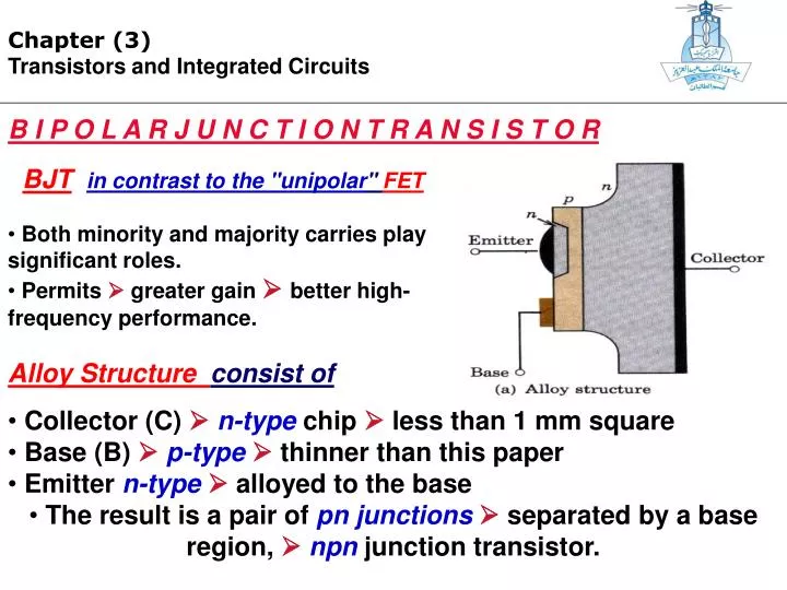
Chapter (3) Transistors and Integrated Circuits. B I P O L A R J U N C T I O N T R A N S I S T O R. BJT in contrast to the "unipolar " FET Both minority and majority carries play significant roles. Permits greater gain better high-frequency performance. Alloy Structure consist of.

E N D
Chapter (3) Transistors and Integrated Circuits B I P O L A R J U N C T I O N T R A N S I S T O R • BJTin contrast to the "unipolar" FET • Both minority and majority carries play significant roles. • Permits greater gain better high-frequency performance. • Alloy Structure consist of • Collector (C) n-type chip less than 1 mm square • Base (B) p-type thinner than this paper • Emittern-type alloyed to the base • The result is a pair of pn junctions separated by a base region, npn junction transistor.
Chapter (3) Transistors and Integrated Circuits • Planar Structure • npnBJT • (n) grown upon a heavily doped (n+) substrate. • oxidation of the surface • window opened to diffuse impurities (P) into the crystal to form the pn junction. • A smaller window for emitter in opened to diffuse emitter region (n). Biasing Parameters BJT C E B VEB VCBiE iC iB
Chapter (3) Transistors and Integrated Circuits Operation • The emitter junction forward biased VEB reduced the barrier at emitter electrons injection into B where they are minority carriers. • The collector junction is reverse biased VCB increase the barrier at C • B is very thinmost electron pass from E to C • The net result transfer electron from E to C. • Large RL insertion in C large voltage voltage amplification • Variation of the base current iBlargeiCcurrent amplification • Switching operation used in digital signal processing.
Chapter (3) Transistors and Integrated Circuits • DC Behavior • E forward C reverse biased. • iE consist electron across npJ holes from B. • g almost unity iE nearly electrons. • avaries from 0.90 to 0.999 where a typical value is 0.98. iC = -aiE + ICBO iB = -iE -iC • Most of these electrons in B diffuse to C B is very narrow. • iC consist of iE and a very small current due to thermally generatedminority carrier ICBO
Chapter (3) Transistors and Integrated Circuits Common - Base Characteristics • CB configuration • B common input E output C. • The emitter-base section forward-biased diode. • Input Characteristics • Input characteristicsFig.( b)similar toFig. (a) diodecharacteristics • The effect of VCB small • +VCB emitter open-circuited IE = 0 • C section reverse-biased junction
Chapter (3) Transistors and Integrated Circuits • Output Characteristics • The collector characteristic reverse bias diode iE = - 5 mA, iC = - aiE@ + 5 mA. • The slope of the curves in Fig C due to an effective increase in aas VCB increases. • a alwaysless 1
Chapter (3) Transistors and Integrated Circuits The common base configuration is not good for practical current amplification
Chapter (3) Transistors and Integrated Circuits
Chapter (3) Transistors and Integrated Circuits • Input and output CECharacteristics • iBdepends on VBEonly . • iB = 0 iC = iCEO • a= 0.98 b= 49, • A very small increase in iB large increase in iC • A verysmall increase in a much greater change in b. Practice Problem 6-3
Chapter (3) Transistors and Integrated Circuits