Download
1 / 25
540 likes | 1.68k Views
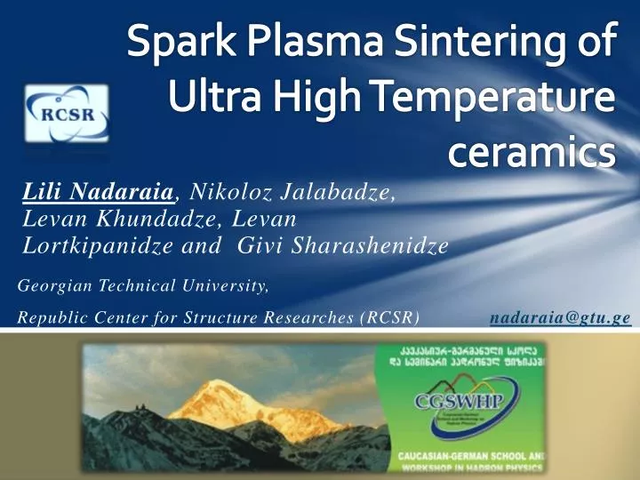
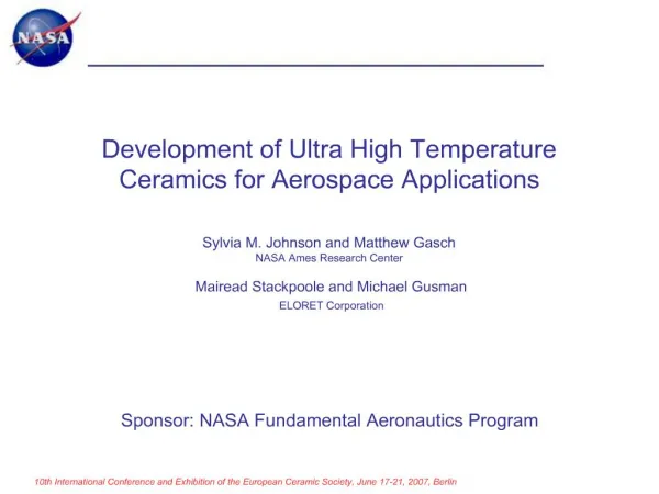
Spark Plasma Sintering of Ultra High Temperature ceramics. Lili Nadaraia , Nikoloz Jalabadze , Levan Khundadze , Levan Lortkipanidze and Givi Sharashenidze. Georgian Technical University, Republic Center for Structure Researches (RCSR). nadaraia@gtu.ge. UHTC. Application. Armor.

E N D
Spark Plasma Sintering of Ultra High Temperature ceramics LiliNadaraia, NikolozJalabadze, LevanKhundadze, LevanLortkipanidze and GiviSharashenidze Georgian Technical University, Republic Center for Structure Researches (RCSR) nadaraia@gtu.ge
Application Armor Nozzles Abrasives UHTC Nuclear applications Refractory applications
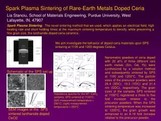
Advantages and disadvantages of spark plasma sintering Advantages of spark plasma sintering: Fast sintering process; Uniform sintering; Low grain growth (nano-grain materials may be prepared); Compaction and sintering stages are combined in one operation; Binders are not necessary; Better purification and activation of the powder particles surfaces; Different materials (Metals,Ceramics, composites) may be processed; High energy efficiency; Easy operation. Disadvantages of spark plasma sintering: Only simple symmetrical shapes may be prepared; Expensive pulsed DC generator is required. Expensive SPS device
Spark plasma between powder particle Fig.1. Scheme of the SPS the process of sintering – PDC - pulsed DC, GD - graphite die, S – powder sample, P – pressure loading, EC- electric current, s – spark, sp – spark plasma and p- powder particles. SPS mechanism by SPS SYNTEX INC Company; (a) I- Flow direction of electrons during DC current, (b) I- Flow directions of electrons during AC current.
DC current shapes Pulse DC current Shape in the developed device: a- at the frequency of 400 Hz, b- during different frequencies (T), different duration pulses (t) and different duration pauses (T-t); Current Shapes to be used after retrofitting the SPS device: during different frequencies (T), different duration pulses (t) and different duration pauses (T-t);
SPS Device Press molds for synthesize nanopowder (a) and sintering dense bodies (b) of composite materials 1-upper plug, 2-lower plug, 3-Matrix.
Self-propagating high-temperature synthesis (SHS), (combustion synthesis CS) Poly SHS Sintering process a: Self-Propagating High-Temperature Synthesis (SHS), b: SPS accompanied with poly SHS. A. G. Merzhanov. 2006, Advances in Science and Technology, 45, 36- 44.
Borides • TiB2 • ZrB2 • HfB2
Titanium Diboride • TiB2 X-Ray and SEM images of Titanium Diborides a- TiB2 powder synthesis at 10000C 1h, b- sintered via SPS at 16000C ; C- SEM image of sintered via SPS at 16000C
Zirconium Diborides X-Ray and SEM images of Zirconium Diborides a- ZrB2 powder synthesis at 10000C 1h, b- sintered via SPS at 16000C ; C- sintered via SPS at17000C • ZrB2 SEM images of Zirconium Diborides sintered via SPS at17000C
Hafnium Diborides X-Ray and SEM images of Hafnium Diborides sintered via SPS at 18000C ; • HfB2
Carbides • TiC • B4C • SiC
Carbides • TiC • SiC X-Ray images of Titanium Carbide sintered via SPS at14000C -3 min; X-Ray images of Silicium Carbide sintered via SPS at18000C -1 min;
Boron Carbide a- XRD pattern of B4C powder (SPS 14000C-3 min) b- SEM image of B4C bulk material (SPS 17000C-10min) • B4C A-XRD patterns of B4C powder materials obtained by standard (a), SPS methods (b) ; B- SEM image of nanopowder B4C obtained by SPS method (14000C-3min).
Composition SPS sintered B4C – SiC (17000C-5min): a-X-ray diffraction pattern; c- SEM image B4C – SiC Sintered via SPS b- SEM image of B4C – SiC powder produce via SPS.
Composition • X –Ray of Ti3SiC2 composition of sintered via SPS at 14500C
Composition • X –Ray and SEM images of TiB2 - TiC composition of sintered via SPS at 14500C TiB2 TiC Vickers hardness 29.5 Gpa
SPS OPERATING MODES WITH RELATIVELY DENSITY Shapes of materials sintered via SPS
Ballistic Testing Test is conducting according Standards of National Institute of Justice (NIJ) (type-IV) Additional energy is absorbed by each successive layer of material in the ballistic panel. http://www.bodyarmornews.com/ Hard Blend (B4C, SiC, B4C-TiB2, B4C-SiC ) Backing material Plastic (Ti-6Al-4V)/textile • Size of the plate -120x120mm; • Size of the plate fragments • 60x60mm; Weight - 50-100g. • The plate presented a package armored with ballistic textile (Kevlar, tvarin, denima);Weight of the package was 0,6 – 0,8 kg; • Fire tests were provided by shooting from the Mosin’s Rifle; • Bullets - armor-piercing • Bullet Mass – 10.8±0,1; • Bullet speed - 869±10 m/sec. • Standard shooting method, distance - 10m towards a plasticine target. Bullet direction
Ballistic testing 120mm BFS 40mm NIJ requirements - Max Back face signature (BFS) depth is 44mm
Conclusion There was developed new technology for manufacturing of nanocrystalline composite materials. Poly SHS process were detect during SPS and were use for UHTC materials fabrication Diborides of transaction metals Ti, Zr, Hf, were produced Nanocrystalline Powders of carbides of metals Ti, Si, and B were obtain after Poly SHS process Effective composition materials TiB2 - TiC, Ti3SiC2, B4C - SiC were developed. Ballistic testing gives promising results and further effort will be directed to improve the characteristics. Modernization of SPS device is undergoing process (replacing of pulse DC current unit with pulse AC current unit). Further work will be directed to detect impacte of DC current at the sintering process and at the materials properties.
Acknowledgement • The part of research described in this presentation was made possible in scope of projects funded by ShotaRustaveli National Science Foundation. • Project # 12/34 Presidential Grants for Young Scientists.
Thank you for attention nadaraia@gtu.ge


![[Sintering]](https://cdn2.slideserve.com/3866196/sintering-dt.jpg)