Download
1 / 33
330 likes | 407 Views
Explore the construction, action, and operating configurations of Bipolar Junction Transistors (BJTs). Learn about transistor classifications, characteristics, parameters, and operating points. Discover the key characteristics through graphs and measurement circuits.

E N D
chapter 2 transistors (BJT) • 2.1 Transistor classification • 2.2 Bipolar junction transistors (BJT) construction • 2.3 Transistor action and operating • 2.4 Quiescent Operating Point • 2.5 Bipolar transistor characteristics • 2.6 Transistor parameters • 2.7 Current gain • 2.8 Typical BJT characteristics and maximum ratings • 2.9 Transistor operating configurations
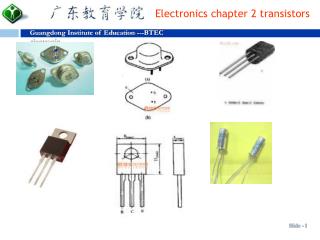
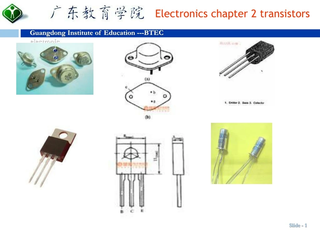
2.2 Bipolar junction transistors (BJT) construction • Bipolar transistors generally comprise n-p-n or p-n-p junctions of either silicon (Si) or germanium (Ge) material. • N: phosphorus or arsenic P: boron or gallium • The junctions are, in fact, produced in a single slice of silicon by diffusing impurities through a photographically reduced mask. • Silicon transistors are superior when compared with germanium transistors in the vast majority of applications
◆The symbols and simplified junction models for n-p-n and p-n-p transistors are shown in Figure 2.3. It is important to note that the base region is extremely narrow. • Figure 2.3 The symbols and simplified junction models for n-p-n and p-n-p transistors
E – Emitter B – Base C - Collector Electronics-BTEC Slide - 6
2.3 Transistor action • ◆In the n-p-n transistor, transistor action is accounted for as follows: • ◆ the base-emitter junction is forward biased and the base-collector junction is reverse biased • ◆ Around 99.5% of the electrons leaving the emitter will cross the Base collector junction and only 0.5% of the electrons will Recombine with holes in the narrow base region. • Figure 2.4 Transistor action of n-p-n transistor
◆the base-emitter junction is forward biased and the base-collector junction is reverse biased • Figure 2.5 Transistor action of p-n-p transistor
2.2.2 leakage current • ◆For an n-p-n transistor, the base-collector junction is reversed biased for majority carriers, but a small leakage current, ICBO , flows from the collector to the base due to thermally generated minority carriers (holes in the • collector and electrons in the base), being present. The base-collector junction is forward biased to these minority carriers. • ◆ With modern transistors, leakage current is usually very small (typically less than 100nA) and in most applications it can be ignored. • ◆ The control of current from emitter to collector is largely independent of the collector-base voltage and almost wholly governed by the emitter-base voltage.
2.2.3 bias and current flow • ◆In normal operation (i.e. for operation as a linear amplifier) the base-emitter junction of a transistor is forward biased and the collector-base junction is reverse biased. • ◆The current flowing in the emitter circuitis typically 100 times greater than that flowing in the base. • Figure 2.7 bias and current flow
Leakage current ICBO 2.2.3 bias and current flow
2.2.4 Transistor operating configurations • ◆Three basic circuit configurations are used for transistor amplifiers. • ◆ These three circuit configurations depend upon which one of the three transistor connections is made common to both the input and the output. • ◆ In the case of bipolar junction transistors, the configurations are known as common emitter, common collector (or emitter follower), and common base. • Figure 2.8 Transistor operating configurations
2.2.5 bipolar transistor characteristics • ◆The characteristics of a bipolar junction transistor are usually presented in the form of a set of graphs relating voltage and current present at the transistors terminals. • Figure 2.9 measurement circuit of bipolar transistor characteristics
◆In this mode, the input current is applied to the base and the output current appears in the collector. • Figure 2.10 Typical input characteristic
◆ Each curve corresponds to a different value of base current. Note the ‘knee’ in the characteristic below VCE =2V. • ◆ Also note that the curves are quite flat. • ◆ For this reason (i.e. since the collector current does not change very much as the collector-emitter voltagechanges) we often refer to this as a constant current characteristic. • Figure 2.11 Output characteristics
◆ Here IC is plotted against IB for a small-signal general-purpose transistor. • ◆ The slope of this curve (i.e. the ratio of IC to IB) is the common-emitter current gain of the transistor. • Figure 2.12 Transfer characteristic
2.2.6 Bipolar transistor parameters • ◆In particular, the three characteristic graphs can be used to determine the following parameters for operation in common-emitter mode:
2.2.6 Bipolar transistor parameters • ◆In particular, the three characteristic graphs can be used to determine the following parameters for operation in common-emitter mode:
2.2.6 Bipolar transistor parameters • ◆In particular, the three characteristic graphs can be used to determine the following parameters for operation in common-emitter mode:
2.2.7 Current gain • ◆We use the symbol hFE to represent the static value of common-emitter current gain. • ◆ Similarly, we use hfe to represent the dynamic value of common-emitter current gain. • ◆ Note that hFE is found from corresponding static values while hfe is found by measuring the slope of the graph. • ◆ Furthermore, most transistor parameters (particularly common-emitter current gain, hfe) are liable to wide variation from one device to the next.
2.2.8 Typical BJT characteristics and maximum ratings • Table 2.2 Transistor characteristics and maximum ratings PTOTmax is the maximum device power dissipation.
2.4 The junction field-effect transistor • Figure 2.13 Conformation of N channel J.F.E.T
2.4 The junction field-effect transistor • N channel JFET • P channel JFET • Figure 2.14 Symbol of JFET
2.4 The junction field-effect transistor • Figure 2.15 Operation of N channel JFET
2.5 Metal-oxide-semiconductor field-effect transistor 2.5.1 depletion-type MOS FET • N channel • P channel Construction of N channel depletion-type MOS FET • Figure 2.16 depletion-type MOS FET
2.5 Metal-oxide-semiconductor field-effect transistor 2.5.2 Enhancement-type MOS FET • N channel • P channel Construction of N channel enhancement-type MOS FET • Figure 2.16 depletion-type MOS FET