Download
1 / 67
6.15k likes | 13.19k Views
CHAPTER 4 :JFET. Junction Field Effect Transistor. Introduction (FET). Field-effect transistor (FET) are important devices such as BJTs Also used as amplifier and logic switches Types of FET: MOSFET (metal-oxide-semiconductor field-effect transistor) Depletion-mode MOSFET

E N D
CHAPTER 4 :JFET Junction Field Effect Transistor
Introduction (FET) • Field-effect transistor (FET) are important devices such as BJTs • Also used as amplifier and logic switches • Types of FET: • MOSFET (metal-oxide-semiconductor field-effect transistor) • Depletion-mode MOSFET • JFET (junction field-effect transistor) • What is the difference between JFET and MOSFET?
Introduction.. (Advantages of FET) • High input impedance (M)(Linear AC amplifier system) • Temperaturestable than BJT • Smaller than BJT • Can be fabricated with fewer processing • BJT is bipolar – conduction both hole and electron • FET is unipolar – uses only one type of current carrier • Less noise compare to BJT • Usually use as logic switch
Disadvantages of FET • Easy to damage compare to BJT • ???
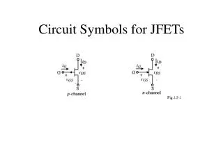
Junction field-effect transistor.. • There are 2 types of JFET • n-channel JFET • p-channel JFET • Three Terminal • Drain – D (Saliran) • Gate -G (Get) • Source – S (Punca)
N-channel JFET • N channel JFET: • Major structure is n-type material (channel) between embedded p-type materialto form 2 p-n junction. • In the normal operation of an n-channel device, the Drain (D) is positive with respect to the Source (S). Current flows into the Drain (D), through the channel, and out of the Source (S) • Because the resistance of the channel depends on the gate-to-source voltage (VGS), the drain current (ID) is controlled by that voltage
P-channel JFET • P channel JFET: • Major structure is p-type material (channel) between embedded n-type materialto form 2 p-n junction. • Current flow : from Source (S) to Drain (D) • Holes injected to Source (S) through p-type channel and flowed to Drain (D)
JFET Characteristic Curve • To start, suppose VGS=0 • Then, when VDS is increased, ID increases. Therefore, ID is proportional to VDS for small values of VDS • For larger value of VDS, as VDS increases, the depletion layer become wider, causing the resistance of channel increases. • After the pinch-off voltage (Vp) is reached, the IDbecomes nearly constant (called as IDmaximum, IDSS-Drain to Source current with Gate Shorted)
ID versus VDS for VGS = 0 V. JFET Characteristic Curve
JFET for VGS = 0 V and 0<VDS<|Vp| Channel becomes narrower as VDS is increased
JFET Characteristic Curve.. • For negative values of VGS, the gate-to-channel junction is reverse biased even with VDS=0 • Thus, the initial channel resistance is higher (in which the initial slope of the curves is smaller for values of VGS closer to the pinch-off voltage (VP) • The resistance value is under the control of VGS • If VGS is less than pinch-off voltage, the resistance becomes an open-circuit ;therefore the device is in cutoff (VGS=VGS(off) ) • The region where ID constant – The saturation/pinch-off region • The region where ID depends on VDS is called the linear/triode/ohmic region
n-Channel JFET characteristics curve with IDSS = 8 mA and VP = -4 V. JFET Characteristic Curve
p-Channel JFET characteristics with IDSS= 6 mA and VP = +6 V.
Operation of n-channel JFET • JFET is biased with two voltage sources: • VDD • VGG • VDD generate voltage bias between Drain (D) and Source (S) – VDS • VDD causes drain current, ID flows from Drain (D) to Source (S) • VGG generate voltage bias between Gate (G) and Source (S) with negative polarity source is connected to the Gate Junction (G) – reverse-biases the gate; therefore gate current, IG = 0. • VGG is to produce depletion region in N channel so that it can control the amount of drain current, ID that flows through the channel
Transfer Characteristics • The input-output transfer characteristic of the JFET is not as straight forward as it is for the BJT. In BJT: • IC= IB • which is defined as the relationship between IB (input current) and IC (output current).
Transfer Characteristics.. In JFET, the relationship between VGS (input voltage) and ID (output current) is used to define the transfer characteristics. It is called as Shockley’s Equation: The relationship is more complicated (and not linear) As a result, FET’s are often referred to a square law devices VP=VGS (OFF)
Transfer Characteristics… • Defined by Shockley’s equation: • Relationship between ID and VGS. • Obtaining transfer characteristic curve axis point from Shockley: • When VGS = 0 V, ID = IDSS • When VGS = VGS(off) or Vp, ID = 0 mA
Transfer Characteristics JFET Transfer Characteristic Curve JFET Characteristic Curve
Exercise 1 Sketch the transfer defined by IDSS = 12 mA dan VGS(off) = - 6
Exercise 1 Sketch the transfer defined by IDSS = 12 mA dan VGS(off) = Vp= - 6 IDSS VGS =0.3VP IDSS/2 VGS =0.5VP IDSS/4
Exercise 2 Sketch the transfer defined by IDSS = 4 mA dan VGS(off) = 3 V
Exercise 2 Sketch the transfer defined by IDSS = 4 mA dan VGS(off) = 3V IDSS IDSS/2 IDSS/4 VP VGS =0.3VP VGS =0.5VP
Answer 2 Answer 2
DC JFET Biasing • Just as we learned that the BJT must be biased for proper operation, the JFET also must be biased for operation point (ID, VGS, VDS) • In most cases the ideal Q-point will be at the middle of the transfer characteristic curve, which is about half of the IDSS. • 3 types of DC JFET biasing configurations : • Fixed-bias • Self-bias • Voltage-Divider Bias
Fixed-bias • Use two voltage sources: VGG, VDD • VGG is reverse-biased at the Gate – Source (G-S) terminal, thus no current flows through RG (IG = 0). + + Vout _ + Vin _ Fixed-bias
Fixed-bias.. • DC analysis • All capacitors replaced with open-circuit Loop 1
Fixed-bias… 1. Input Loop • By using KVL at loop 1: VGG + VGS = 0 VGS = - VGG • For graphical solution, use VGS = - VGG to draw the load line • For mathematical solution, replace VGS = -VGG in Shockley’s Eq. ,therefore: 2. Output loop - VDD + IDRD + VDS = 0 VDS = VDD – IDRD 3. Then, plot transfer characteristic curve by using Shockley’s Equation
Example : Fixed-bias • Determine the following • network: • VGSQ • IDQ • VD • VG • VS
Graphical solution for the network Draw load line for:
Self-bias • Using only one voltage source
DC analysis of the self-bias configuration. Q point for VGS
Mathematical Solutions: • Replace in the Shockley’s Equation: • By using, quadratic equation and formula, choose value of ID that relevant within the range (0 to IDSS): nearly to IDSS/2 • Find VGS by using ;also choose VGS that within the range (0 to VP)