Download
1 / 33
330 likes | 355 Views
Explore an integrated debugging environment for FPGA-based signal processing systems. Learn about high-level simulation, HDL/RTL simulation, and native FPGA execution methods. Dive into testing tools like Xilinx ChipScope Pro and System Generator HW-in-the-loop. Discover hands-on hardware debugging techniques, drawbacks of on-FPGA execution, and a proposed solution for extensive debugging directly on the hardware platform. Understand the essential features of the environment for robust design exploration with user-driven control.

E N D
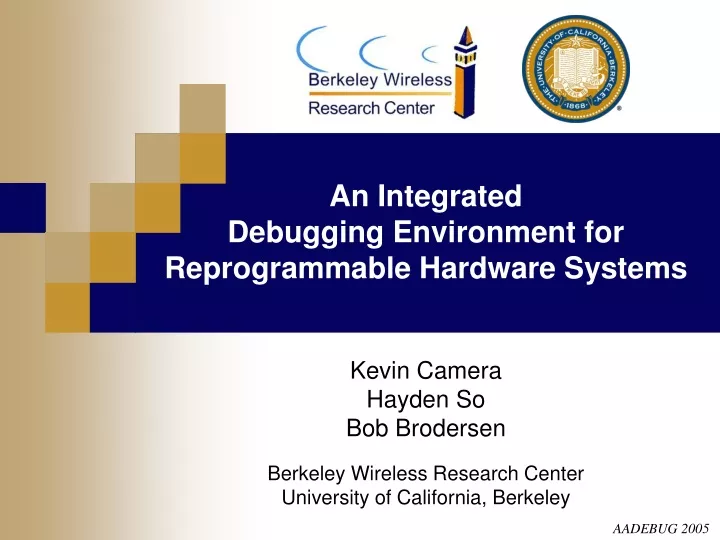
An IntegratedDebugging Environment forReprogrammable Hardware Systems Kevin CameraHayden SoBob Brodersen Berkeley Wireless Research CenterUniversity of California, Berkeley AADEBUG 2005
Outline • Motivation • Existing platform • Existing design/verification flow • Proposed solution • Environment features • Walkthrough • Implementation strategy
Application Domain • Direct-mapped, reprogrammable hardware systems • FPGA-based signalprocessing andsupercomputingarrays
Superior power, computation, and cost efficiency than any processor-based solution, due to direct mapping of algorithms FPGA Computing Benefits Chang, Wawrzynek, Brodersen; ISCA ‘05
BEE2: 2nd Berkeley Emulation Engine • (5) Xilinx V2P100 per board • ~100K logic cells • 2 PowerPC405 cores • 444 dedicated multipliers • 1MB on-chip SRAM • 3.125Gb/s duplex links • (4) DDR2 banks per FPGA • 72 bits per bank with ECC • Up to 12.8 (DDR400) or 17 (533DDR) GB/s bandwidth • Up to 4GB capacity
BEE Design Flow • Design entry is in the Matlab/Simulink environment • Graphical, library based; also allows custom HDL • Typical FPGA path to physical implementation • HDL synthesis and place and route • Hierarchy is flattened in each pass (non-modular flow)
Design Verification Methods • High-level functional simulation • HDL/RTL simulation • Native FPGA execution Complexity,Accuracy
High-level Functional Simulation • Design executionin Matlab/Simulink • Intended to becorrect byconstruction • Fastest software-based simulation • Powerful and convenient algorithm exploration
Drawbacks of High-level Simulation • Even with high level of abstraction, vastly slower than hardware • Trend is worsening with increased FPGA capacity • Doesn’t cover any side-effects or requirements of the backend tool chain
HDL/RTL Simulation • Varying levelsof accuracy • Access toarbitraryinternal signals • But, simulation speed is even slower • Parameterization/Iteration is much harder
Native FPGA Execution • Runs at full speed of hardware • Three tools for on-FPGA testing: • Xilinx ChipScope Pro • System Generator HW-in-the-loop • Good old-fashioned signal probing
Xilinx ChipScope Pro • Inserts BRAM cores into design and binds to JTAG • Captures selected signals and provides trigger conditions • Signals of interest must be chosen in advance • Captured state is limited by available BRAM • Any changes require tool flow re-iteration
System Generator HW-in-the-loop • Allows hardware itself to accept and process data from Simulink via JTAG • Arbitrary number of data elements can be accessed as “ports” • Very powerful tool, but features limited process control
Hands-on Hardware Debugging • Most accurate method for finding timing-related bugs in a “production” system • Tradeoffs are all too well-known: • Complex equipment • Limited probing pins • A priori signal output • Limited input options
Drawback of On-FPGA Execution • Place and route time is a major bottleneck • Complete run is needed for every design change • Increasingly problematic due to larger FPGA capacity
Proposed Solution • Enable extensive debugging and design exploration functionality directly on the hardware platform • Vastly superior execution time for today’s large-scale computing challenges • Exploit the spatial resources of the hardware to assist in debugging • Essentially a -g switch to the hardware design flow • Minimize or eliminate iterations through implementation flow
Caveats • Final timing of design will not be preserved • Critical path will definitely be increased,but 106 is a lot of headroom • Timing-driven implementation still needed once verification is complete • Significantly more FPGA capacity and memory will be needed • Acceptable for scalable BEE-like platforms and for modular, tiled algorithms
Essential Features of Environment • Robustly parameterized library components with soft configuration • Design exploration without tool iterations • Readily accessible variable contents • Reading and writing of any values by user • Complete user-driven control over process execution • Single-step, bursts, breakpoints, assertions
1: Parameterized Library • Number of bits • Saturate / Wrap • Binary point position • Microarchitecture • Library components provide configuration parameters as inputs, which can be set by variables • Allows runtime modification of function properties, including precision, range, and latency • Enables design-space exploration at hardware speed, plus correction of configuration errors without re-implementation
2: Data Management • Ability to dynamically observe any variable’s value at the user’s request • Ability to overwrite a variable’s value at runtime and continue operation • Ability to rewind system state within the bounds of buffer capacity
2: Data Management Requirements • Too expensive to re-implement the hardware to expose new data • All variables are streamed into local and off-chip storage, such as DRAM and disks • Unlike software, hardware is highly parallel, and often deeply pipelined • Memory requirements could be extreme • Can be offset by hierarchical memory architecture and/or periodic sampling
3: Process Control • Inherit the most useful features of software debuggers like GDB • Cycle-by-cycle (single-step) execution • Breakpoints (either state dependent, or fixed cycle count) • Implemented using multiple clock domains and clock buffer control • Already available for use on BEE2
Walkthrough: Design • Use specialized libraries to provide soft configuration • Integrates directly into the existing BEE2 tool flow
Walkthrough: Tagging • User tags signals of interest with debugging testpoints • Defines a variable name • Defines other parameters of interest for data observation • Also includes breakpoints and assertions
Walkthrough: Stitching • “Stitcher” updates the design before entering back-end tool flow • Inserts logic as needed for debug functions • Instantiates PowerPC core and master controller • Adds underlying connections to route data
Walkthrough: Runtime • User can monitor variables and control process execution from remote client • Embedded PowerPC software provides a thin service layer • Client is fully integrated with Matlab and Simulink input description
Control Architecture on BEE2 Control FPGA Network PPC ClockBufferLogic 100MHz User Defined (~1-10MHz) Single-step Clockdomains Breakpointinterrupt Control DRAM User FPGA Inserted Logic UserDesign
Stitching • Stitcher traverses the design hierarchy and: • Replaces debugging component placeholders with necessary logic • Creates a simple route from all variables to off-chip storage devices • During execution, the stitcher records: • A mapping between variable names and their physical variable unit in hardware • The latency within the variable routing network
Variable Control Unit (VCU) • Inserted in place of each variable block in design • Automatically implied for every state variable in a state machine • Combination of local buffers and off-chip DRAM • Exact memory allocation is subject to experimentation
Debug Controller (DC) • Interface between all variable and assertion instances, the runtime user shell, and process control “services” • Regulates the system clock both for exceptions and to prevent variable storage overflows
Future Work • Complete infrastructure for BEE2 • Extensive experiments with variable memory • Efficient methods for variable routing • Storage requirements and hierarchy • Time/Space tradeoffs for periodic sampling • Generalize framework to define concepts such as variable priorities, multiple debug levels, and extensions to text-based languages