Download
1 / 42
460 likes | 557 Views
Explore thin film deposition methods like CVD, ALD, PVD, and more available at NUFAB's cutting-edge cleanroom facility, aiding in advanced material research and development.

E N D
Thin Film Deposition at NUFAB CVD, ALD and Beyond John Ciraldo and William Mohr
Introduction • Northwestern University Micro/Nano Fabrication Facility • 6000 foot Class-100 cleanroom • 4 Bays: • Characterization • Lithography • Wet Bench Processing • Etch & Deposition • Staff of 6 scientist & engineers • Full process & development support • Located on ground floor of Tech F-wing Thin Film Deposition at NUFAB: CVD, ALD, & Beyond
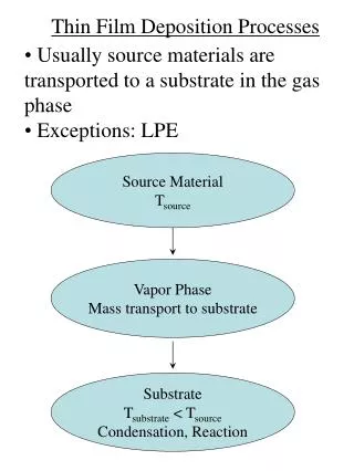
Thin Film Deposition • PVD • Physical Vapor Deposition • Thermal Evap., MBE, e-Beam Evap., Sputter, PLD… • CVD • Chemical Vapor Deposition • PECVD,LPCVD,MWCVD, MOCVD… • Some other stuff • ALD, spin coating, electroplating… Thin Film Deposition at NUFAB: CVD, ALD, & Beyond
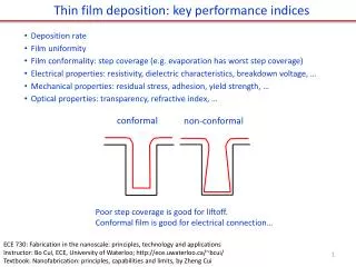
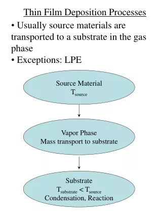
PVD vs CVD • Physical Vapor Deposition (PVD) relies on physical processes to vaporize solid materials • Chemical Vapor Deposition utilizes reactions between one or more precursors and in-situ gases • Precipitate is deposited on substrate • CVD tends to be associated with higher temperature depositions and higher depositions rates Thin Film Deposition at NUFAB: CVD, ALD, & Beyond
Thermal Evaporation • Chamber is evacuated to high vacuum • Source material typically placed in W crucible • Source material is heated to sublimation, allowing for deposition • Reasonably good step coverage • Can be controlled somewhat through geometry • Spitting is possible for some materials • Deposition can be quite fast • Poor process tunability • Materials limited by thermal properties Thin Film Deposition at NUFAB: CVD, ALD, & Beyond
Thermal Evap At NUFAB • Denton Vacuum Explorer 14 • Accommodates wafer sizes up to 6” • Substrate heating up to 200°C • Three 200kVA shielded sources • Recipes proved for: • Multiple metals, high rate Cu and Au Thin Film Deposition at NUFAB: CVD, ALD, & Beyond
Molecular Beam Epitaxy (MBE) • Special case of thermal evaporation where Knudson (effusion) cells are used and throw distance is typically increased • Generally limited to epitaxy • Performed at UHV • Not available at NUFAB Thin Film Deposition at NUFAB: CVD, ALD, & Beyond
E-Beam Evaporation • Special case of evaporation where the source is heated by an e- beam • Generally line-of-sight coverage • Efficient use of source materials • Well suited for lift-off processes • Not ideal for 3D structures • Compound materials may decompose under high temperatures Thin Film Deposition at NUFAB: CVD, ALD, & Beyond
E-Beam Evaporation At NUFAB • AJA ATC-2036-E System • Accommodates substrates up to 6” • 6 pockets for source material, 2 user configurable • Water-cooled, rotatable substrate holder • Substrate heating to 200°C • Staff-provided processes • Al, Ni, Cr, Au, Ag, Mo, Ti, W… Thin Film Deposition at NUFAB: CVD, ALD, & Beyond
Sputtering • Physical erosion via ion bombardment • Comes in many ‘flavors’ • RF, DC, Pulsed-DC, HiPIMS… • Suitable for most solid materials • Generally good conformality • Somewhat process tunable • Provides challenges for lift-off • Processes are highly tunable Thin Film Deposition at NUFAB: CVD, ALD, & Beyond
Sputtering How does it work? • Plasma ignition via electrical excitation and mechanical interactions • Ions, typically argon, are accelerated towards the target material • Near the target, the ions are ‘steered’ by a strong magnetic field • Upon ion collision, atoms are ejected from target, with some depositing on substrate Thin Film Deposition at NUFAB: CVD, ALD, & Beyond
Sputtering How does it work? • Plasma ignition via electrical excitation and mechanical interactions Thin Film Deposition at NUFAB: CVD, ALD, & Beyond
Sputtering NUFAB Capabilities • NUFAB has two sputtering systems • Both systems: • AJA Orion 8 systems • Up to 8” substrate (4” above 350 °C) • Up to 850°C Substrate heating • RF substrate biasing • +/- 2% thickness uniformity • Sputter I is ‘workhorse’ • most flexibility in allowed materials • RF, DC, Pulsed DC and HiPIMS capabilities • User installed targets • Sputter II is high purity system • RF, DC and Pulsed DC capabilities • Staff installed targets • Recently added gold and platinum sources • Staff-written processes: • Ultra fast, multiple source processes for Cu and reactive SiO2 • ITO, Bi, Fe, Au, Pt… Thin Film Deposition at NUFAB: CVD, ALD, & Beyond
Pulsed Laser Deposition (PLD) • Sputtering, but with lasers • Source material is ablated form target using high-power laser pulsed • Can be prone to spitting, particulate formation and globular depositions • Due to vapor quenching, can be used to study metastable material phases • Not available at NUFAB Thin Film Deposition at NUFAB: CVD, ALD, & Beyond
Thin Film Deposition • PVD • Physical Vapor Deposition • Thermal Evap., MBE, e-Beam Evap., Sputter, PLD… • CVD • Chemical Vapor Deposition • PECVD,LPCVD,MWCVD, MOCVD… • Some other stuff • ALD, spin coating, electroplating… Thin Film Deposition at NUFAB: CVD, ALD, & Beyond
Chemical Vapor Deposition • Deposition typically occurs due to reactions at the substrate surface • Not a single technique, but a family of techniques • Prone to high rate depositions for thin and thick films • Far too many variants for a single talk Thin Film Deposition at NUFAB: CVD, ALD, & Beyond
Low Pressure CVD (LPCVD) • Functionally similar to APCVD (atmospheric pressure CVD) • Common technique for silicates • Pressures on order of 75-750 mTorr • Lower pressure dramatically improved mass transport characteristics (slows them) • Improved step coverage • CVD is thermally driven • Typical temperatures in the range of 600-1100°C Thin Film Deposition at NUFAB: CVD, ALD, & Beyond
Plasma Enhanced CVD (PECVD) • Chemical interactions induced via electrical stimulation, rather than thermal • Allows for significantly lower substrate temperatures during deposition • Typical excitation is RF, but may be DC • Very fast depositions realizable • 10s to 100s of nm/min possible • At very high rates, uniformity may be sacrificed • Good conformality for structured wafers Thin Film Deposition at NUFAB: CVD, ALD, & Beyond
LPCVD vs PECVD Thin Film Deposition at NUFAB: CVD, ALD, & Beyond
LPCVD At NUFAB • Recipes for standard and low-stress Si3N4 • Both recipes stoichiometric • Dichlorosilane (SiH2Cl2) based recipes, ammonia reducer • 4” Wafer capability, with ability to load many wafers simultaneously • 25 wafers/carrier • Processing temperature: 835°C • Fully automated processes Thin Film Deposition at NUFAB: CVD, ALD, & Beyond
PECVD At NUFAB • STS (SPTS) LpX CVD tool • Configured for 4” substrates • Small substrates easily accommodated with carrier wafer • Equipped with loadlock and automated transfers • Fully automated processes • Silane based processes • Recipes for silicon oxide, silicon nitride and polysilicon • Typical process temperate is 300°C • Can accommodate 200-400°C processes • Dual excitation sources for stress control in nitride films • HF: 13..56 MHz, LF: 380kHz • Staff-Provided recipes for Low stress SiO2, low stress Si3N4, polysilicon at multiple dopant concentrations, low temp processes… Thin Film Deposition at NUFAB: CVD, ALD, & Beyond
Overview of Techniques • Conventional deposition techniques • MOCVD • ALD • Less Conventional • Parylene • Spin on Glass (SOG) Thin Film Deposition and NUFAB CVD, ALD, & Beyond
MOCVD Overview • Metal Organic Chemical Vapor Deposition • Typically used for III-V or II-VI materials • GaN, InGaAs, AlGaAs, GaAs, InP, SiC, AlN • Homoepitaxy and heteroepitaxy • Typically used in for creating photonic and power and RF devices • Pros: • High throughput • Epitaxy • Large variety of materials • Easy to change between materials • Sharp interfaces • Good uniformity • Cons: • Expensive • Can have extremely hazardous and or expensive sources • Process needs to be closely monitored • Not at NUFAB Thin Film Deposition and NUFAB CVD, ALD, & Beyond
MOCVD: Metal Organics • Metal Organics • Ligand • Metal • Typical Sources • Trimethyl Aluminum • Trimethyl Gallium • Triethyl Gallium • Trimethyl Indium Ligand Metal Thin Film Deposition and NUFAB CVD, ALD, & Beyond
MOCVD: Hydrides • Hydrides • Typical Sources • NH3 • AsH3 • PH3 • SiH4 • Si2H6 Thin Film Deposition and NUFAB CVD, ALD, & Beyond
MOCVD: Principal of Operation Hydride manifold Wafer Hydrides Chamber Gas Injection Carrier Gas Susceptor planetary rotation Pump and Exhaust system MO manifold Heater Metal Orgainics Thin Film Deposition and NUFAB CVD, ALD, & Beyond
MOCVD: Principal of Operation Thin Film Deposition and NUFAB CVD, ALD, & Beyond
MOCVD: Principle of Operation • Metal Organics and Hydrides Mix in reaction chamber (500 – 1200C) • Chemicals pyrolyze in chamber due to heat • Resulting metal lands on surface and random walks until a step is found • Organic is removed through the exhaust Thin Film Deposition and NUFAB CVD, ALD, & Beyond
ALD Overview • Atomic Layer Deposition • Typically used when: • High uniformity is required • Need to coat sidewalls of device • Very tight thickness tolerances • Typically lower temperature deposition as compared to other CVD processes • Pros: • Large variety of materials • Easy to change between materials • Sharp interfaces • Good uniformity • Cons: • Low throughput • Very slow • Can have extremely hazardous and or expensive sources Thin Film Deposition and NUFAB CVD, ALD, & Beyond
ALD: Applications • Optical • Antireflection • Optical filters • Photonics • Transparent Conductors • Electronics/MEMS • Gate dielectrics • Gate electrodes • Diffusion barriers • DRAM • Flexible electronics • Other • Nanotubes • Powders • Wear/corrosion resistant coatings • Fuel cells/catalysis Thin Film Deposition and NUFAB CVD, ALD, & Beyond
ALD: Sources • Same precursors as MOCVD • Additional precursors are also available based on material, temperature, cost restraints • Typical reducers for ALD • H2O • N2 plasma • O3 (Ozone) • O2 plasma • NH3 • NH3 plasma Thin Film Deposition and NUFAB CVD, ALD, & Beyond
ALD: Principle of Operation • Discrete steps "Thermal and Plasma-Enhanced Atomic Layer Deposition on Powders and Particles Geert Rampelberg, VéroniqueCremers, Delphine Longrie, Davy Deduytsche, Johan." Thin Film Deposition and NUFAB CVD, ALD, & Beyond
ALD: Principle of Operation Oxidizer/ Reducer manifold Plasma Injection Oxidizer/ Reducer Wafer Chamber Carrier Gas Heated chuck no rotation needed Pump and Exhaust system MO manifold Metal Organics Thin Film Deposition and NUFAB CVD, ALD, & Beyond
ALD: NUFAB Capabilities • ArradianceGEMStar XT-P • Up to 6” substrates • Chamber Heats to 350C • Platten Heats up to 500C • Four slots for precursors • Can be changed by Staff with 48 hr notice • Can create Ar, O2, H2, NH3 plasma • Mechanical rotation for coating powders • Films currently available: • Al2O3, HfO2, TiO2, Pt, ZnO, SiO2 Thin Film Deposition and NUFAB CVD, ALD, & Beyond
Parylene: Overview • CVD process that creates biocompatible coating of devices for medical industry • Also used to protect electronics from the environment • Pros: • Directly coats surfaces at room temperature with high uniformity, high repeatability, and pinhole free • Chemically stable and biocompatible • Barrier to oxygen and moisture • Fungal resistant • Thermal mechanically stable • Electrical isolation of samples • Adheres well to most surfaces • Cons: • Limited only to parylene • Must be vacuum compatible Thin Film Deposition and NUFAB CVD, ALD, & Beyond
Parylene: NUFAB Capabilities • SCS Labcoter2 Parylene Deposition System • Two systems: I and II • Fixture Rotation • Process parameters optimized for Parylene C • provided by NUFAB • 1g of Parylene yields ~ 1µm of film Thin Film Deposition and NUFAB CVD, ALD, & Beyond
Parylene: Principle of Operation Gas distribution Substrate holder Furnace Rotates Cold Trap Heats to 690C Vaporizer Monomer Gas Dimer Solid Dimer Gas Polymer Pump Thin Film Deposition and NUFAB CVD, ALD, & Beyond
Spin On Glass (SOG): Overview • Method for depositing SiO2 without a vacuum chamber • Used for barrier layers and for electrical isolation • Biodegradable • Able to deposit at a range of thicknesses depending on spin speed and viscosity • Used in electronic industry as replacement for PECVD for electrical isolation and in medical field as biodegradable/biocompatible barrier • Silicate (e.g. Na2SiO2 + water + ethanol + acetone + isopropanol) Thin Film Deposition and NUFAB CVD, ALD, & Beyond
Spin On Glass (SOG): Procedure • Attach substrate to spin coater • Apply SOG • Set spinner to 3000 RPMs for 40 sec • Bake at 200C for 60s • Repeat procedure for a thicker coating • Bake at 400C for 30min to solidify completly Thin Film Deposition and NUFAB CVD, ALD, & Beyond
Spin On Glass (SOG): NUFAB Capabilities • Properties after baking for 200C for 60sec • Thicknesses: 200 nm • Index of refraction: 1.41 • Properties after baking for 400C for 30min • Thickness: 170nm • Index of refraction: 1.34 • Volume Resistivity 5x10¹³Ωcm • Surface Resistance 2x10¹² Ω/ Thin Film Deposition and NUFAB CVD, ALD, & Beyond
Review Thin Film Deposition and NUFAB CVD, ALD, & Beyond