Download
1 / 40
410 likes | 614 Views
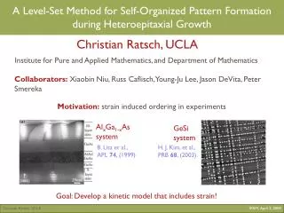
Growth, Structure and Pattern Formation for Thin Films Lecture 3. Pattern Formation. Russel Caflisch Mathematics Department Materials Science and Engineering Department UCLA. www.math.ucla.edu/~material. Outline. Directed self-assembly A possible route to improved microelectronics

E N D
Growth, Structure and Pattern Formation for Thin FilmsLecture 3. Pattern Formation Russel Caflisch Mathematics Department Materials Science and Engineering Department UCLA www.math.ucla.edu/~material U Tenn, 4/30/2007
Outline • Directed self-assembly • A possible route to improved microelectronics • Thin film growth with strain • Coupling the level set method & atomistic strain solver • Dependence of kinetic coefficients on strain • Pattern formation over buried dislocation lines • Alignment of stacked quantum dots U Tenn, 4/30/2007
Outline • Directed self-assembly • A possible route to improved microelectronics • Thin film growth with strain • Coupling the level set method & atomistic strain solver • Dependence of kinetic coefficients on strain • Pattern formation over buried dislocation lines • Alignment of stacked quantum dots U Tenn, 4/30/2007
Maintaining Moore’s Law for Device Speed • Radically different devices will be required • Feature sizes approaching the atomic scale • 50nm by 2010 • Wavelength (visible light) = 400nm • New device physics • photonics, spintronics, quantum computing • New device structures • Massively parallel nanoscale structures • Constructed through self-assembly (bottom-up) or directed self-assembly • Too small for conventional lithography (top-down) • New approaches to lithography are emerging, e.g., using plasmons (edge waves) U Tenn, 4/30/2007
Approaches to Self-Assembly or Directed Self-Assembly • Solid-state structures on thin films • Quantum wells, wires and dots • Molecular systems • Self-assembled monolayers (SAMs) • Bio/organic systems • E.g., DNA structures • Block Copolymer systems U Tenn, 4/30/2007
Block Copolymer Systems • Composites of different polymeric strands • Attraction/repulsion between strands leads to segregation and patterns • Currently used to improve precision of lithographic patterns From Paul Nealey, U. Wisconsin U Tenn, 4/30/2007
Self-Assembled Monolayers • Chemically-assembled molecular systems • If each molecule has switching properties, the resulting system could be a massively parallel device Molecular switch Stoddart, UCLA SAM construction U Tenn, 4/30/2007
DNA Structures and Patterns • Complex interactions of DNA strands can be used to create non-trivial structures • The structures can be pieced together to make patterns Ned Seeman, NYU U Tenn, 4/30/2007
Solid-State Quantum Structures • Quantum wells (2D) • “perfect” control of thickness in growth direction • Lasers, fast switches, semiconductor lighting • Quantum wires (1D) • Various strategies for assembly • Quantum dots (0D) • Self-assembled to relieve strain in systems with crystal lattice mismatch (e.g., Ge on Si) • Difficult to control geometry (size, spacing) ANU InAs on InP Grenier et al. 2001 Ge/Si, Mo et al. PRL 1990 U Tenn, 4/30/2007
Directed Self-Assembly of Quantum Dots • Vertical allignment of q dots in epitaxial overgrowth (left) • Control of q dot growth over mesh of buried dislocation lines (right) AlxGa1-xAs system GeSi system B. Lita et al. (Goldman group), APL 74, (1999) H. J. Kim, Z. M. Zhao, Y. H. Xie, PRB 68, (2003). In both systems strain leads to ordering! U Tenn, 4/30/2007
Outline • Directed self-assembly • A possible route to improved microelectronics • Thin film growth with strain • Coupling the level set method & atomistic strain solver • Dependence of kinetic coefficients on strain • Pattern formation over buried dislocation lines • Alignment of stacked quantum dots U Tenn, 4/30/2007
How do we combine Levelset code and strain solver? A straightforward way to do this: • This introduces kinks (and we have not yet studied the significance of this …. ) • Nevertheless, the relevant microscopic parameters at every grid point can now be varied as a function of the local strain. • Christian Ratsch (UCLA & IPAM) U Tenn, 4/30/2007
Energetic Description of Prepatterning • Strain affects the energy landscape for a crystal • Ea = attachment energy = energy min above crystal atoms • Et = transition energy = energy of barriers between energy min • Kinetic parameters • Diffusion coefficient D depends on Et - Ea • Variation in Ea→ “thermodynamic drift velocity” vt towards lower energy • We propose these as the connection between strain and patterns • Theory of pattern formation and self-assembly is needed! Et Ea U Tenn, 4/30/2007
GaAs(100) (a semiconductor) E. Penev, P. Kratzer, and M. Scheffler, Phys. Rev. B 64, 085401 (2001). How does strain affect the parameters in our model? Density-functional theory (DFT) has been used to study strain dependence of surface diffusion D Ag/Ag(111) (a metal) Etrans Ead Energy barrier for surface diffusion Ratsch et al. Phys. Rev. B 55, 6750-6753 (1997). U Tenn, 4/30/2007
How does strain affect the parameters in our model, cont.? • Stain also changes the detachment rate Ddet • No DFT results for strain dependence of Ddet are known (but calculations are in progress …. ); but is is plausible that strain makes binding of edge atom less stable. • Assume that energy barrier for detachment is reduced by a strain energy: Thus, detachment rate Ddetis enhanced upon strain: • Preliminary results suggest that the dependence of Ddet is more important for ordering of island sizes, while dependence of D is more important for ordering of location. U Tenn, 4/30/2007
Diffusion Coefficient D and Thermodynamic Drift Velocity vt for Variable Ea and Et • Diffusion coefficient D • comes from the energy barrier Et - Ea • Equilibrium adatom density • depends on the attachment energy Ea • and • Same formulas for D and v from atomistic model U Tenn, 4/30/2007
Replace diffusion constant by matrix: • D = D0 exp(-(Etr-Ead)/kT) Diffusion in x-direction Diffusion in y-direction Possible potential energy surfaces • Diffusion equation: no drift • Velocity: drift • Nucleation Rate: Modifications to the Level Set Formalism for non-constant Diffusion Etr Ead U Tenn, 4/30/2007
Outline • Directed self-assembly • A possible route to improved microelectronics • Thin film growth with strain • Coupling the level set method & atomistic strain solver • Dependence of kinetic coefficients on strain • Pattern formation over buried dislocation lines • Alignment of stacked quantum dots U Tenn, 4/30/2007
Directed Self-Assembly of Quantum Dots Motivation: Results of Xie et al. (UCLA, Materials Science Dept.): Growth on Ge on relaxed SiGe buffer layer Dislocation lines are buried below Spatially varying strain field leads to spatially varying diffusion Hypothesis: Nucleation occurs in regions of fast diffusion Level Set formalism is ideally suited to incorporate anisotropic, spatially varying diffusion without extra computational cost H. J. Kim, Z. M. Zhao, Y. H. Xie, PRB 68, (2003). U Tenn, 4/30/2007
Creation of Dislocation Network • Layered system • Substrate Si (001) • 800Å Si.85Ge.15 buffer layer • 100Å Si capping layer • Anneal to relax buffer layer • Dislocation network • substrate/buffer interface • Mixed edge/screw type • Q dots grow on top of 900Å layer • Ge or SiGe • Along slip plane from buried dislocations Q Dots U Tenn, 4/30/2007
Q Dots and Dislocation Network • TEM • Q dots on surface • Buried dislocation lines --- is location of slip plane at surface → are Burgers vectors Kim, Chang, Xie J Crystal Growth (2003) U Tenn, 4/30/2007
Growth over Buried Dislocation Lines • Ge coverage • 4.0 Å • 4.5 Å • 5.0 Å • (d) 6.0 Å U Tenn, 4/30/2007
Model for Growth • Prescribe variation in Ea, Et • Variable D and vt • Perform growth using LS method • Nucleation occurs for larger values Dρ2 • Pattern formation in islands positions • Seeds positions for quantum dots • Niu, Vardavas, REC & Ratsch PRB (2006) • Diffusion equation: • Diffusion coefficient (matrix): • D = D0 exp(-(Etr-Ead)/kT) • Thermo drift velocity • Nucleation Rate: U Tenn, 4/30/2007
Experiment by Xie et al., UCLA First part: assume isotropic, spatially varying diffusion Only variation of transition energy; constant adsorption energy fast diffusion slow diffusion • Islands nucleate in regions of fast diffusion U Tenn, 4/30/2007
Kinetic limit Thermodynamic limit Etrans Etrans Ead Ead Nucleation in region of slow diffusion (but high adatom concentration), dominated by drift Nucleation in region of fast diffusion Nucleation rate ~ Variation of adsorption or transition energy U Tenn, 4/30/2007
Etrans Etrans Ead Ead Variation of both, adsorption and transition energy In phase Out-of phase U Tenn, 4/30/2007
Comparison with Experimental Results Results of Xie et al. (UCLA, Materials Science Dept.) Simulations U Tenn, 4/30/2007
Comparison with Experimental Results Results of Xie et al. (UCLA, Materials Science Dept.) Simulations U Tenn, 4/30/2007
From islands to wires For islands that are well aligned, due to prepatterning, further growth can lead to monolayer wires U Tenn, 4/30/2007
Outline • Directed self-assembly • A possible route to improved microelectronics • Thin film growth with strain • Coupling the level set method & atomistic strain solver • Dependence of kinetic coefficients on strain • Pattern formation over buried dislocation lines • Alignment of stacked quantum dots U Tenn, 4/30/2007
Vertically Aligned Quantum Dots Q. Xie, et al. ( Madhukar group), PRL 75, (1995) B. Lita et al. (Goldman group), APL 74, (1999) U Tenn, 4/30/2007
b a a b a Repeat Capping and Growth of N Super layers n capping layers of Si Ge Si Substrate Simulation of stacked quantum dots • Growth of islands on substrate without strain (constant diffusion and detachment) • Fill in capping layer “by hand” • Calculate strain on top of smooth capping layer • Modify microscopic parameters for diffusion and detachment) according to strain • Run growth model • Repeat procedure • Niu, Luo, Ratsch U Tenn, 4/30/2007
LS Growth with PES Calculated from Strain Repeat Capping and Growth N rounds LS Growth with PES Calculated from Strain Get Sxx and Syy by Using Strain Code n Layers of Capping Si Ge Island LS Growth with Artificial PES (prepatterning) Si Substrate U Tenn, 4/30/2007
a b a b a Repeat Capping and Growth N rounds n Layers of Capping Si Si Substrate U Tenn, 4/30/2007
AlxGa1-xAs system B. Lita et al., APL 74, (1999) Ordering of stacked quantum dots • Spacing and size of stacked dots becomes more regular U Tenn, 4/30/2007
9 capping layers 1 capping layer 2 capping layers Thickness dependence of vertical ordering • We find an optimal thickness of capping layer for ordering U Tenn, 4/30/2007
Nucleation of islands after one capping layer Effect of capping layer thickness n • Capping layer • Thin • nucleation at bdry • Moderate • nucleation at center • Thick • random nucleation n=0 n=1 n=2 n=3 n=4 n=5 U Tenn, 4/30/2007
Growth of island after nucleation • Capping layer • Thin • misshaped islands • Moderate • circular islands • regularly placed • Thick • displaced islands n=0 n=1 n=2 n=3 n=4 n=5 U Tenn, 4/30/2007
60 30 60 Nucleation rate as a function of capping layer thickness U Tenn, 4/30/2007
Conclusions • Island dynamics/level set method • Combined to simulate strained growth • Kinetic parameters assumed to have strain dependence • Directed Self-Assembly • Growth over a network of dislocation lines • Alignment of stacked quantum dots • Unsolved problems • Growth mode selection (e.g., formation of wetting layer) • Pattern design and control (e.g., quantum dot arrays) • Optimizing material (and device) properties U Tenn, 4/30/2007