Download
1 / 23
230 likes | 469 Views
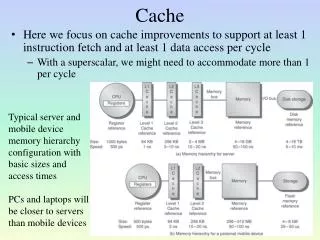
Cache. Cache Design for Performance Comparison Intel Pentium 4 Motorola PowerPC G4 Trends Glossary. Memory Hierarchy / Locality. Design for Performance. Size High performance All memory the system can cache The design of chipset Type Unified/Separated Data+Instruction cache.

E N D
Cache • Cache Design for Performance • Comparison • Intel Pentium 4 • Motorola PowerPC G4 • Trends • Glossary
Design for Performance • Size • High performance • All memory the system can cache • The design of chipset • Type • Unified/Separated Data+Instruction cache
Design for Performance • Size • Mapping • Replacement algorithms • Write policy • Block size • Number of caches
Design for Performance • Write Policy • Write back • One extra data bit • Higher performance than write through • Write through • multiple CPUs can monitor main memory traffic to keep local to CPU cache up to date • Lots of traffic and slow-down write (buffer = big help) • * Multi processors : data consistancy in different caches
Design for Performance • Block size • In general miss rate block size • Miss penalty block size • Number of caches • Cost, performance
Pentium 4 L2 cache options • 256 KB L2 integrated cache, 400 Mhz system bus • 512 KB L2 integrated cache 400 or 533 Mhz front side bus
P4 L1 Execution Trace Cache • stores up to 12K decoded micro-ops in the order of program execution • increases performance by circumventing decoder in main execution loop • efficient storage: branched instructions are not stored
PowerPC G4 • Motorola’s MPC7457 Processor: 1.3 GHz • Dual processor G4s share cache between processors • General market availability: Q4 2003
PowerPC G4: L1 Cache • Harvard architecture: split between data and instruction cache • 32 KB 8-way set associative • Pseudo-LRU replacement algorithm • 32 byte (8 word) L1 cache block • 4 instructions per clock cycle (instruction) & 4 words per clock cycle (date) • Cache way locking allows performance alogorithms and code to be locked into the cache. • Write back/through programmed per page or per block
PowerPC G4: L2 Cache • On-chip, unified instruction and data cache • 512 KB, 8-way set associative. Runs at processor speed. • 32 bytes/clock cycle communication with L1 cache • Write back/through programmed per page or per block • Pseudo-LRU replacement algorithm • Two 32 byte sectors per line • Twice the amount as previous G4s
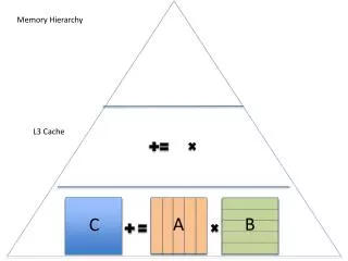
PowerPC G4: L3 Cache • 2 MB off-chip L2 cache using DDR SDRAM • Runs at speeds up to 500 MHz • 1, 2, or 4 MB SRAM space • 1 or 2 MB cache space • 1 MB or 2 MB sectored line size • Dedicated bus to processor (4 GB/sec) • Dual processors: each has own L3 cache
G4 enhancement plan • Pipelining: Increase #, keep pipelines short • Small # of simultaneous instructions in various stages of execution (up to 16) • execute instructions in parallel, move them off chip in as few cycles as possible.
Drawbacks: G4 plan • more execution units added to handle decoding • Fewer instructions pipelined at any given time
Benefits: G4 Plan • Shorter miss penalties (min. 4 clock cycles) • Introduce Mitigating Factor: • Added L3 cache with 64 bit bus • Increased size of execution units speeds performance “wider and shallower”
P4 Enhancement Plan • Innovative cache implementation • “Narrow, but deep” pipelining: • higher clock speeds • Deep scheduling queues to prevent pipeline “bubbles”
Drawbacks: P4 plan • Larger miss penalties (min. 19 clock cycles) • due to longer pipelining • Longer slower pipelines require complicated scheduling • No L3 cache
Benefits: P4 Plan • Trace Cache significantly improves throughput to execution cycle • Faster clock speeds overall
Sources • http://www.intel.com • http://www.apple.com/powermac/architecture.html • “MPC7457 RISC Microprocessor Hardware Specs” http://e-www.motorola.com/webapp/sps/library • “Motorola – PowerPC G4” http://www.geek.com • “Cache Latencies of the MPC7450” http://www.motorola.com • “Motorola Delivers….” http://www.us.design-reuse.com/news/news4852.html • “The Fundamentals of Cache” http://www.systemlogic.net/articles/00/10/cache/page2.php