Download
1 / 26
270 likes | 653 Views
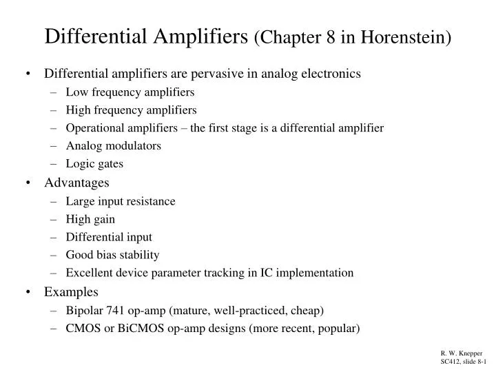
Differential Amplifiers (Chapter 8 in Horenstein). Differential amplifiers are pervasive in analog electronics Low frequency amplifiers High frequency amplifiers Operational amplifiers – the first stage is a differential amplifier Analog modulators Logic gates Advantages

E N D
Differential Amplifiers (Chapter 8 in Horenstein) • Differential amplifiers are pervasive in analog electronics • Low frequency amplifiers • High frequency amplifiers • Operational amplifiers – the first stage is a differential amplifier • Analog modulators • Logic gates • Advantages • Large input resistance • High gain • Differential input • Good bias stability • Excellent device parameter tracking in IC implementation • Examples • Bipolar 741 op-amp (mature, well-practiced, cheap) • CMOS or BiCMOS op-amp designs (more recent, popular) R. W. Knepper SC412, slide 8-1
Amplifier With Bias Stabilizing Neg Feedback Resistor • Single transistor common-emitter or common-source amplifiers often use a bias stabilizing resistor in the common node leg (to ground) as shown below • Such a resistor provides negative feedback to stabilize dc bias • But, the negative feedback also reduces gain accordingly • We can shunt the common node bias resistor with a capacitor to reduce the negative impact on gain • Has no effect on gain reduction at low frequencies, however • Large bypass capacitors are difficult to implement in IC design due to large area • Conclusion: try to avoid using feedback resistor R2 in biasing network R. W. Knepper SC412, slide 8-2
Differential Amplifier Topology • In contrast to the single device common-emitter (common-source) amplifier with negative feedback bias resistor of the previous slide, the differential ckt shown at left provides a better bypass scheme. • Device 2 provides bypass for active device 1 • Bias provided by dc current source • Device 2 can also be used for input, allowing a differential input • Load devices might be resistors or they might be current sources (current mirrors) • The basic differential amplifier topology can be used for bipolar diff amp design or for CMOS diff amp design, or for other active devices, such as JFETs R. W. Knepper SC412, slide 8-3
Differential Amplifier with Two Simultaneous Inputs • The differential amplifier topology shown at the left contains two inputs, two active devices, and two loads, along with a dc current source • We will define the • differential mode of the input vi,dm = v1 – v2 • common mode of the input as vi,cm= ½ (v1+v2) • Using these definitions, the inputs v1 and v2 can be written as linear combinations of the differential and common modes • v1 = vi,cm + ½ vi,dm • v2 = vi,cm – ½ vi,dm • These definitions can also be applied to the output voltages • Differential mode vo,dm = vo1 – vo2 • Common mode vo,cm = ½ (vo1 + vo2) • Alternately, these can be written as • vo1 = vo,cm + ½ vo,dm • vo2 = vo,cm – ½ vo,dm R. W. Knepper SC412, slide 8-4
Bipolar Transistor Differential Amplifier • Q1 & Q2 are matched (identical) NPN transistors • Rc is the load resistor • Placed on both sides for symmetry, but could be used to obtain differential outputs • Io is the bias current • Usually built out of NPN transistor and current mirror network • rn is the equivalent Norton output resistance of the current source transistor • Input signal is switching around ground • Vref = 0 for this particular design • Both sides are DC-biased at ground on the base of Q1 and Q2 • vBE is the forward base-emitter voltage across the junctions of the active devices • Since Q1 and Q2 are assumed matched, Io splits evenly to both sides • IC1 = IC2 = Io/2 R. W. Knepper SC412, slide 8-5
Small-Signal Model Analysis for Single Input Diff Amp • Consider transistor Q2 with grounded base • dc small-signal model shown in top-left figure • Use the test voltage approach to calculate Q2’s input impedance looking into emitter • Using KCL equations, we can write itest = vtest/r – oib2 where ib2 = - vtest/r • Rearranging and solving for vtest/itest, we have rth2 = vtest/itest = r/(o + 1) = ~ r/o = 1/gm2 • Generally gm2 is large, causing rth2 to act like an ac short • Consider transistor Q1 with Q2 replaced by rth2 • Since rth2 is much smaller than rn (output impedance of Io), we will neglect rn • Writing KCL, we have vin = ib1r1 + ib1(o + 1) rth2 = ib12 r1 • where we assumed r1= r2 • We can now find vout as a function of vin vout = - ic1Rc = - oibRc = - ovinRc/2r1= - ½ gmRcvin • where we have used gm = o/r1 • Small signal gain Av = vout/vin = - ½ gmRc R. W. Knepper, SC412, slide 8-17
Bipolar Diff Amp with Differential Inputs • At left is a bipolar differential amplifier schematic having two inputs that are differential in nature, i.e. equal in magnitude but opposite in phase • The differential input v1 – v2 = va(t) – (-va(t)) = 2va(t) • The common mode input = [va + (-va)]/2 = 0 • A small-signal model for the diff amp is shown below, where the Tx output collector resistance ro is assumed to be >> RC (in parallel) and is neglected • We can derive the small-signal gain due to the differential input by applying KVL to loop A va(t) – (-va(t)) = 2va(t) = ib1r1 – ib2r2 = 2ib1r • since ib1 = -ib2 and r1= r2 • Or, ib1 = va(t)/r and ib2 = - va(t)/r R. W. Knepper SC412, slide 8-18
Bipolar Diff Amp with Differential Inputs (continued) • Solving for the output voltages we can obtain • vo1 = -ic1RC = - oib1RC = - (o/r)va(t)RC and v02 = + (o/r)va(t)RC • We can now find the gain with differential-mode input and single-ended output or with differential-mode input and differential output Adm-se1 = v01/vidm = -gmRC/2 and Adm-se2 = + gmRC/2 Adm-diff = (v01 – v02 )/ vidm = - gmRC • Since corresponding currents on the left and right side of the differential small-signal model are always equal and opposite, implying that no current ever flows throw rn • Node E acts as a “virtual ground” • If the output resistances of Q1 and Q2 are low enough to require keeping them in the analysis, we simply replace RC with the parallel combination of RC||ro for transistor Q1 and Q2 R. W. Knepper SC412, slide 8-19
Small-Signal Model of BJT Diff Amp with CM Inputs • The figure below is the small-signal model for the diff amp with common-mode inputs • v1 = v2 = vb(t) and vicm = ½ (v1 + v2) = vb(t) • The common-mode currents from both inputs flow through rn as shown by the two loops • in = 2(o + 1) ib1 = 2 (o + 1) ib2 • and therefore, vb = ibr + 2(o+ 1)ibrn or ib = vb/[r + 2(o+ 1)rn] • The collector voltages can be found as • v01 = v02 = - oRCvb/[r + 2(o+ 1)rn] = ~ - gmRCvb/ [1 + 2gmrn] • The common-mode gain with single-ended output is given by • Acm-se1 = Acm-se2 = vo1/vicm = vo2/vicm = - gmRC/[1 + 2gmrn] = ~ -RC/2rn • The common-mode gain with differential output is Acm-diff = (vo1 – vo2)/vicm = 0 • Do Example 8.1, p. 488 R. W. Knepper SC412, slide 8-20
BJT Diff Amp Circuit with Both Diff & CM Inputs • The example below illustrates the principle of superposition in dealing with both differential mode and common mode inputs to a diff amp • v1 = vx cos 1t + vy sin 2t and v2 = vx cos 1t – vy sin 2t • Using the definitions of differential mode and common mode inputs, respectively, vidm = v1 – v2 = 2vy sin 2t and vicm = (v1 + v2)/2 = vx cos 1t , • we can obtain vo1 = Adm-se1 vidm + Acm-se1 vicm = - oRC [(vy/ r) sin 2t + (vx/{r + 2 (o+ 1) rn}) cos 1t] • The expression for v02 is similar except that the first term (differential mode) has a minus sign • Note that the common mode output is reduced by the factor (o+ 1) in the denominator R. W. Knepper SC412, slide 8-21
Common-Mode Rejection Ratio • In a differential amplifier we typically want to amplify the differential input while, at the same time, rejecting the common-mode input signal • A figure of merit Common Mode Rejection Ratio is defined as CMRR = |Adm|/|Acm| • where Adm is the differential mode gain and Acm is the common mode gain • For a bipolar diff amp with differential output, the CMRR is found to be CMRR = |Adm-diff|/|Acm-diff| = |- gmRC| / 0 = infinity • In the case of the bipolar diff amp with single-ended output, CMRR is given by CMRR = |Adm-se|/|Acm-se| = | ½gmRC| / | oRC/[r + 2(o+ 1)rn]| = [r + 2(o+ 1)rn]/2r = ~ orn/r = gmrn = ICrn/VT = Iorn/2VT • since o = gmr and VT is defined as kT/q • CMRR is often expressed in decibels, in which case the definition becomes • CMRR = 20 log (|Adm|/|Acm|) R. W. Knepper SC412, slide 8-22
BJT Diff Amp Input and Output Resistance Input Resistance: • For differential-mode inputs, the input resistance can be found as • rin-dm = (v1 – v2)/ib1 = (va – (-va)) / (va/r) = 2var/va = 2r • For common-mode inputs, the input resistance is quite different • rin-cm = ½(v1 + v2)/ib1 = vb / [vb /(r+ 2(o+ 1)rn)] = r + 2(o+ 1)rn Output Resistance: • For differential outputs, we can use the test voltage method (below) for deriving the output resistance where all inputs are set to zero • Since ib1 and ib2 are both zero, we have itest = vtest/(RC + RC) = vtest/2RC or rout-diff = 2RC • For single-ended outputs, rout-se = RC || ro = ~ RC R. W. Knepper SC412, slide 8-23
Bipolar Diff Amp Biasing Considerations • A bipolar differential amplifier with ideal current source and resistor loads is shown • It is assumed that components are matched sufficiently such that bias current Io is split evenly between the left and right-hand legs • Node E will take a voltage value such that IC1 = IC2 = Io/2 when v1 = v2 = 0 • By using the Ebers-Moll dc model for the NPN transistors, we can determine the voltage at node E IE = IEO [exp (qVBE/kT) – 1] = IEO exp (qVBE/kT) = Io/2 or, VBE = (kT/q) ln (IE/IEO) • Typically, VBE = 0.75-0.85 V in modern NPN transistors • It is important to design RC such that vout never drops so low so as to force Q1 or Q2 into saturation. R. W. Knepper SC412, slide 8-24
BJT Diff Amp with Simple Resistor Current Source • The simplest approach to building a current source is with a resistor • Given that node E is one VBE drop below GND, we can choose RE to provide the desired bias current Io • RE = (0 – VBE – VEE) / Io • Preventing saturation in Q1 and Q2 provides an upper bound for RC • RC ~ < (VCC – 0)/(Io/2) = 2 VCC / Io • Look at Example 8.3 in text. • Do problem 8.31 in class. R. W. Knepper SC412, slide 8-25
Example 8.3: Diff Amp with Complete Bias Design • Design Conditions • Differential-mode, single-ended gain > = 50 • Common-mode, single-ended gain < = 0.2 • Completed design is shown above • In class Exercise: 8.4, 8.5, & 8.6 R. W. Knepper SC412, slide 8-26
BJT Diff Amp with BJT Current Source • The expression for common-mode gain on slide 8-20 (-RC/2rn) shows that in order to reduce Acm, we want to make the effective impedance of the current source very high • Using a resistor to generate the current source limits our design options in making rn (RE in this case) high • An alternate method of generating Io is to use an NPN transistor current source similar to that shown at the left • Q3 is an NPN biased in the forward active region so that rn (given by the inverse slope of the collector characteristics) is very high • RA and RB form a voltage divider establishing VB = VEE x RA/(RA + RB) where VEE is <0 • The voltage across RE can be used to find Io • VRE = VB – Vf – VEE • Io = (VB – Vf – VEE)/RE is the bias current provided to the diff amp R. W. Knepper SC412, slide 8-27
Small Signal Model of BJT Current Source Transistor • Find the small-signal resistance looking into the collector of Q3 on slide 8-27 diff amp • If RE were = 0, then the solution becomes simply ro, since the incremental base current ib3 would, in fact, be 0 • With a finite feedback resistor RE, we need to use KVL and KCL to derive an expression for rn (See Example 8.4 in text) • Apply a test current itest and find vtest • Obtain v3 by applying KVL to the 3 left-most resistors to obtain ib3 and multiply by r3 v3 = -itest RE r3 /[RE + r3 + RP] • If we multiply this result by gm3 and substract from itest, we obtain io3 which can be used to find vo3 by multiplying by r03 vo3 = itest{1 + gm3RE r3 /[RE + r3 + RP]}ro3 • ve can be found as (itest + ib3) x RE ve = itest (r3 + RP) RE/(RE + r3 + RP) • Adding vo3+ ve = vtest, we obtain rn = vtest/itest rn = RE || (r3 + RP) + r03 [1 + oRE/(RE+ r3+RP)] Do Exercise 8.8 and 8.9 in class. R. W. Knepper SC412, slide 8-28
Bipolar Current Mirror Circuit • A method used pervasively in analog IC design to generate a current source is the current mirror circuit • In the bipolar design arena, the method is as follows: • A reference current is forced through an NPN transistor connected as a base-emitter diode (base shorted to collector), thus setting up a VBE in the reference transistor • This VBE voltage is then applied to one or more other “identical” NPN transistors which sets up the same current Iref in each one of the bias transistors • As long as the bias transistor(s) is (are) identical to the reference transistor, and as long as the bias transistor(s) is maintained in its normal active region (where collector current is independent of the collector-emitter voltage), then the current in the bias transistor(s) will be identical to the current in the reference transistor. • Variations on the basic current mirror circuit can be used to generate 2X or 3X or maybe 10X the original reference current by using several bias NPN transistors in parallel • Or alternately, by using an emitter that has 2X or 3X or 10X emitter stripes and is otherwise identical to the reference transistor • Advantages • One reference current generator can be used to provide bias to several stages • Very high incremental output impedance can be obtained from the current mirror • The technique can be used in both bipolar and in CMOS/BiCMOS technologies R. W. Knepper SC412, slide 8-29
Bipolar Current Mirror Bias Circuit Design • Design procedure: • Given RA and the IC vs VBE characteristics of the NPN reference device, we can determine IA, or • Given the desired IA and the IC vs VBE characteristics of the NPN reference device, we can choose RA • We can find IA by dividing the voltage drop across RA by the resistance value • IA = (VCC – VBE1 – VEE) / RA • Assuming that the two base currents are small, we can say IA = Iref • Because of the current mirror action, the VBE1 set up in Q1 to sustain current Iref will be equal to VBE2, the base-emitter voltage in Q2 • Therefore, Io = Iref = IA • Note: corrections for IB1 and IB2 can easily be made is needed • Note 2: Q2 must be maintained in its forward active region R. W. Knepper SC412, slide 8-30
BJT Diff Amp with Current Mirror Bias (Ex. 8.5) • Design Objectives: • Diff amp with 1.5 mA in each leg • 5V drop across load resistors • VCC = +10V, VEE = -10V • Design Procedure: • Set Io = IA = 3 mA • RA = (0 – VBE = VEE)/3mA = 3.1K • where we used VBE = 0.7 volt • RC1 & RC2 can be found as follows: • RC1 = RC2 = 5V/1.5 mA = 3.3K • Check VCE of Q2, Q3, and Q4 to see if they are in normal active region • VC = VCC – 1.5 mA x 3.3K = 5V • VE = 0 – VBE = -0.7V • VCE = 5 – (-0.7) = 5.7V for Q2 and Q3 • For Q2 VCE = -0.7V – (-10) = -9.3V • Calculate power in each device • PQ3 = PQ4 = 1.5mA x 5.7V = 8.6 mW • PQ2 = 3 mA x 9.3V = 28 mW • PQ1 = 3 mA x 0.7V = 2.1 mW R. W. Knepper SC412, slide 8-31
BJT Current Mirror Feeding 2-stage Diff Amp • The example below shows a 2-stage bipolar diff amp fed from two current sources with a single current mirror • Reference current 0.93mA is determined by placing (0 – VBE – VEE) across a 10K bias resistor • The reference current is used for the first differential stage with 0.47 mA on each leg • The second differential stage is to have double the bias current of the first stage • This is accomplished by using two bias NPN transistors in parallel giving 1.86 mA bias current with 0.93 mA flowing on each leg (Q7 and Q8) • Check the VCE of each device to check for normal active region and calculate power in circuit. • The total circuit power is found by computing the sum of the three current source currents multiplied by the source-sink voltage differential for each. • Q1: 0.93mA x 10V = 9.3mW • Q2: 0.93mA x 20V = 18.6mW • Q3/Q4: 1.86mA x 20V = 37.2 mW • Total circuit power = 65.1 mW R. W. Knepper SC412, slide 8-32
Bipolar Widlar Current Source • A special use of the current mirror is the Widlar Current Source (shown at left) • A resistor in the emitter of Q2 is used to reduce the current Io in Q2 to a value less than that in Q1 • Io can be set to a very small value by increasing the R2 value • Design procedure: • As in the standard current mirror, we can find Iref as follows: Iref = (VCC – VEE – VBE1)/RA • But, in contrast to the standard current mirror, VBE2 will not be equal to VBE1 VBE1 = VBE2 + IE2R2 • Using the Ebers-Moll model for emitter current IE = IEO (exp[VBE/VT] – 1) = ~ IEO exp[VBE/VT] • We can invert this expression and insert it into the above equation for VBE1 to obtain IE2 = (VT/R2) ln(IE1/IE2) = Io = (VT/R2) ln(Iref/Io) • Since this is not a closed form solution, an iterative approach can be used to solve for Io by starting with a best guess. • Example iteration procedure: • Assume that Iref = 1 mA and R2 = 500 ohms. Guess Io inside ln term. Find LHS Io. • Initial guess = 0.5 mA, then Io = 0.036mA • Try a guess of 0.2 mA, then Io = 0.083mA • Try a guess of 0.1mA, then Io = 0.119mA • Try a guess of 0.11mA, then Io = 0.114mA Close enough!! R. W. Knepper SC412, slide 8-33
Small-Signal Model for Widlar Current Source Q1 • The incremental output impedance (looking into Q2 collector) of Widlar Current Source is similar to the expression derived for the BJT current source (slide 8-28) except that RP must be replaced by the incremental resistance at the base of Q1 • From the model below, the incremental resistance at the base of Q1 is given by r1 || 1/gm1 || ro1 || RA = ~ [r1/(o1 + 1)] || RA • Thus, the output impedance seen looking into the collector of the Widlar Current Source is given by rn = R2 || (r2 + RP) + r02 [1 + o2R2/(R2+ r2+RP)] • where the above expression is to be used in place of RP • However, with a number of approximations and using the relation IoR2/VT= ln (Iref/Io), the expression may usually be simplified to rn = r02 [1 + ln (Iref/Io)] • Look over Example 8.9 in text. R. W. Knepper SC412, slide 8-34
Amp. Multietapa con Diferenciales • El circuito de la figura 2 funciona como un amplificador rudimentario. La salida del amplificador diferencial está derivada en una forma de una sola terminal y alimentada a un seguidor de voltaje que sirve como un acoplador de salida. Suponga que la BF de cada transistor ocurre en el rango de 50 a 200. • Encuentre el punto de operación aproximado de cada transistor del circuito para un valor supuesto de Vf=0.7V. • Identifique las entradas V+ y V-. • Determine las expresiones para las ganancias diferencial y común del amplificador.
Amp. Multietapa con Diferenciales Utilicé donde sea apropiado aproximaciones de ingeniería, y suponga que están pareados todos los BJT, determineLos valores aproximados del punto de polarización de cada uno de los transistores. La ganancia de voltaje en pequeña señal Vo/(V1-V2).
Diseño Con Amplificadores Diferenciales • Diseñe un amplificador diferencial a BJT que cumpla con las especificaciones siguientes: • Adm=100, • CMRR>60dB, • Rango de excursión diferencial en las terminales de salida de por lo menos 3 v pico. • rin-dif >1k • rout-se<1k, • Están disponibles canales de alimentación de mas o menos 10 v