Download
1 / 13
140 likes | 297 Views
This project proposes a gas sputter deposition system for depositing conductive and dielectric materials on various substrates. The system consists of six main components and aims to optimize functionality and design through physical modeling, theoretical analysis, computer simulations, and design optimization. The project includes component fabrication, testing, and system assembly with a hello-world demonstration of multilayer conductive wires.

E N D
Project Proposal SputteringDeposition System Reginald Bryant Xu Sun MAS 961, Spring 2004
Presentation Overview • Project Overview • System Description • Functionality • Design Process • Hello-World Demonstration
I. Project Overview • A Gas Sputter Deposition System is proposed. Basic function is deposition of conductive and dielectric materials (including Al, SiN…) on various substrates (including Si, SiO). • The Advantage of this system over the existing technology is:
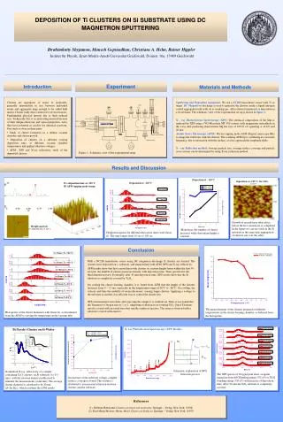
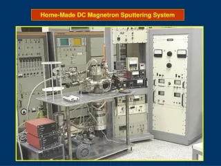
System Description • There are primarily SIX components in the system: 1. Target System ----- target material layer to be deposited on the substrate 2. Shutter & Masks ----- programmable deposition pattern 3. Plasma Sources ----- plasma hitting and kicking off target particles 4. Movement Control System ----- XYZ movement of target layer and/or shutter masks 5. Sample Holding System ----- fixed plane to hold sample at the bottom of enclosure 6. Enclosure & Pump ----- Entire system is enclosed in rare gas environment with temp, pressure control
1. Target System • Function: ----- Holding target heads • Design Parameters: ----- Quality of target layer (existing standard deposition technology) ----- Topology of heads We plan to make only two target heads for prototyping
2. Shutter and Masks • Function: ----- Deposition pattern one-use masks or programmable reusable shutter • Design Parameters: -----The complexity and resolution of the pattern
3. Plasma Source • Function: ----- Use high microwave voltage to generate Argon plasma. Electrons in plasma heat target material and kick them out. • Design Parameters: ----- Power level of plasma source, control electrical network.
4. Movement Control System • Function: ----- Control the movement of deposition-head including X-Y-Z- axis. • Design Parameters: ----- Movement precision and operation complexity ----- Good to compatible with existing prototyping machine such as Modella, laser cutter or waterjet
5. Sample Holding System • Function: ----- holding the sample substrate • Design Parameters: ----- easy to operate
6. Enclosure and Pump • Function: ----- Include all the parts of system in a vacuum enclosure to ensure a clean environment. Temperature control. • Design Parameter: ----- Reasonable vacuum, temperature
Functionality • Deposition Scaling from 10 microns to 10 nanometers. • Monolithic Passive components • Monolithic Active components • Multilayer chip
Design Process • Physical Modeling • Theoretical analysis of required temperature, pressure, geometry • Computer simulations of deposition process • Design Optimization -- Different schemes, e.g. target heads movable or masks movable or both • Component fabrication -- Target heads, shutter/masks, enclosure, electronic parts • Component Test -- • System Assembly
Hello-world demonstration • Multilayer conductive wires sandwiched between insulators. • Test the electrical quality, i.e. continuity of the wires and isolation of different layers