Download
1 / 16
160 likes | 393 Views
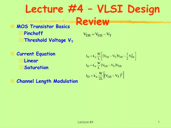
Lecture #4 – VLSI Design Review. MOS Transistor Basics Pinchoff Threshold Voltage V T Current Equation Linear Saturation Channel Length Modulation. b. •. •. 1.5V. c. •. a. At ‘a’. At ‘b’. At ‘c’. For NMOS. For PMOS. |V. |. GS. R. on. |V. | > |V. |. GS. T. |V.

E N D
Lecture #4 – VLSI DesignReview • MOS Transistor Basics • Pinchoff • Threshold Voltage VT • Current Equation • Linear • Saturation • Channel Length Modulation Lecture #4
b • • 1.5V c • a At ‘a’ At ‘b’ At ‘c’ Lecture #4
For NMOS For PMOS Lecture #4
|V | GS R on |V | > |V | GS T |V | < |V | GS T Switch Model of CMOS Transistor Lecture #4
VDD VIN VOUT Inverter DC Operation Voltage Transfer Characteristic Vout Vin Vout V OH Vin = Vout Vth Switching Threshold V OL Vin V V OL OH Nominal Voltage Levels Vth =? Lecture #4
V in 50% t t t pHL pLH V out 90% 50% 10% t t t f r Delay Definitions Lecture #4
CMOS Inverter Steady State Response VDD VDD RON V = V OH DD VOUT VOUT V = 0 OL Threshold Voltage V = f(R , R ) RON th onn onp VIN = VDD VIN = 0 Lecture #4
CMOS Circuit Fabrication Process Steps for Patterning through Photolithography Optically project the shadow of a pattern on to the chip and transfer the pattern to the chip Lecture #4
Polysilicon Gate Field Oxide (Thick Oxide) Gate Oxide (Thin Oxide) NMOS Transistor Lecture #4
Patterning Silicon Si - Substarate Silicon Di-oxide Lecture #4
Lithography Process used to transfer patterns to each layer of IC. Lithography sequence steps: Designer: - Drawing the layer patterns on a layout editor Silicon Foundry: - Mask generation from the layer patterns in the design data base - Printing: transfer the mask pattern to the wafer surface - Process the wafer to physically pattern each layer of the IC Lecture #4
Process Steps Lecture #4
Photoresist Oxide Layer Silicon Wafer Process steps for Patterning Grow Crystal Saw Bare silicon Wafer 4-12” dia <1mm Silicon Wafer Thermal Grow Oxide Layer Oxidation SiO2 1m Oxide Layer Silicon Wafer Spin coating with Photoresist –1mm Light Sensitive organic polymer Acid-resistant Soluble once exposed to UV Light Lecture #4
Oxide Layer Silicon Wafer Pattern formed on a glass plate (Mask) Transparent & Opaque regionsPositive Photoresist Non exposed regions hardened higher resolution Expose to Ultraviolet Light Exposed soluble (hardened) Lecture #4
Soluble photoresist is chemically removed (etching) using HF acid Oxide Layer Silicon Wafer Silicon Wafer Silicon Wafer Etching continued to remove SiO2 High-temp. plasma removes hardened photoresist Pattern formed Lecture #4
Si - Substarate Patterned Silicon Lecture #4