Download
1 / 32
460 likes | 1.39k Views
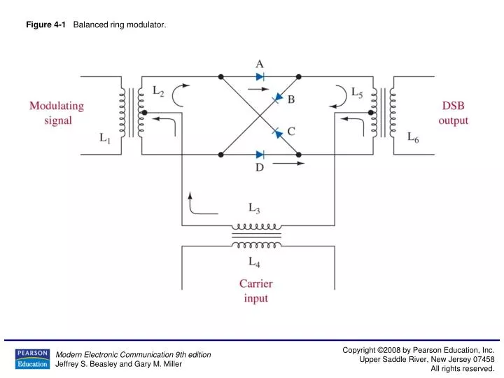
Figure 4-1 Balanced ring modulator. Figure 4-2 The Analog Devices AD630 balanced modulator/demodulator. (Courtesy of Analog Devices.). Figure 4-2 (continued) The Analog Devices AD630 balanced modulator/demodulator. (Courtesy of Analog Devices.).

E N D
Figure 4-2 The Analog Devices AD630 balanced modulator/demodulator. (Courtesy of Analog Devices.)
Figure 4-2(continued) The Analog Devices AD630 balanced modulator/demodulator. (Courtesy of Analog Devices.)
Figure 4-2(continued) The Analog Devices AD630 balanced modulator/demodulator. (Courtesy of Analog Devices.)
Figure 4-9 SSB generator-filter method. (From the ARRL Handbook, courtesy of the American Radio Relay League.)
Figure 4-13 Linear power amplifier. (Courtesy of Microwaves and RF.)
Figure 4-14 AM, DSB, and SSB waves from sinusoidal modulating signals.
Figure 4-18 SSB receiver. (From the ARRL Handbook, courtesy of the American Radio Relay League.)
Figure 4-18 (continued) SSB receiver. (From the ARRL Handbook, courtesy of the American Radio Relay League.)
Figure 4-20 Checking for carrier leakthrough with an oscilloscope.
Figure 4-21 Single-sideband signal with and without carrier leakthrough.
Figure 4-22 Checking carrier suppression with a spectrum analyzer.
Figure 4-23 Carrier suppression as seen on a spectrum analyzer.
Figure 4-27 A multiplier plus SSB filter as implemented with Electronics WorkbenchTM Multisim.
Figure 4-28 The double-sideband output spectrum for the multiplier circuit.
Figure 4-29 The multiplier circuit with the lower sideband removed.