Download
1 / 32
320 likes | 477 Views
Fcal sensors & electronics. Alternatives and investigations. 7 sessions in 2 days:. 1-Introduction session 1: Physics and Beam diagnostic using beamcal 2- Session 2 : integration, vacuum issues. 3- Session 3 : Lumical and Beamcal issues 4- session 4: FCAL Electronics and readout.

E N D
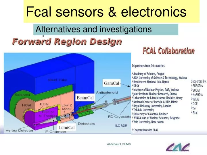
Fcal sensors & electronics Alternatives and investigations Abdenour LOUNIS
7 sessions in 2 days: 1-Introduction session 1: Physics and Beam diagnostic using beamcal 2- Session 2 : integration, vacuum issues 3- Session 3 : Lumical and Beamcal issues 4- session 4: FCAL Electronics and readout Saturday 1- Beamcal and Lumical Mechanics 2- Background estimations and algorithms 3- Discussion and closeout session Abdenour LOUNIS http://ilcagenda.linearcollider.org/conferenceDisplay.py?confId=2285
Angular coverage 150 mrad 30 mrad lumical Beamcal Gamcal 5 mrad IP 180 m 3,050 m 3,650 m Geometry and position 30 X0 Abdenour LOUNIS
BeamCal: W-sensor Sandwich BeamCal: 5 < θ < 28 mrad 20 < R(mm) < 165 Length = 30 X0 (3.5mm W + .5mm sensor) Molière radius= 1 cm Space forelectronics Abdenour LOUNIS Pad size : ½ RMoliere
The BeamCal detector • purpose: • Detection of electrons/photons at low angle • Beam diagnostics from beamstrahlung electrons/positron pairs • Shielding of Inner Detector • Extend the sensitive region to lowest polar angles (hermeticity) Two photon cross section Background 105 times higher than SUSY Cross section Abdenour LOUNIS
The BeamCal detector • Two photon events is the most serious background in many physics searchs (Beyond SM) (missing energy and missing momentum) • Very important feature of beamcal is to separate high energy electron with P~P beam and pile up of low energy beamstrahlung pairs Example of Physics signal SUSY : smuon production And missing energy Background signal : 2 photons events may fake signal « in case of electron escape » Abdenour LOUNIS
e+ e- e+e-pairs from beamstrahlung are deflected into the BeamCal Layer 6 Beamstrahlung: Photons and e+e- pairs E deposit and Irradiation • High energy deposition (inner layers of thebeamcal) 105 e+e- pairs depositing up to 10 TeV/bunch crossing • ~ 100 MRad per year Abdenour LOUNIS • response within ms
Challenging Project To built a High Precision device, High occupancy, High radiation level and Fast electronic readout innovation in design techniques Recall • BeamCal structure • 2 end caps • 30 Silicon – Tungsten sandwiched layers per cap • 1512 channels per layer • Total channel count: 90,720 • At 32 channels per chip, this implies 2836 chips Abdenour LOUNIS
Sensor options • Silicon radiation Hard • GaAs • Diamond pCVD , ScCVD Look for best performances in terms of : Signal yield stability , long-term behavior charge collection efficiency charge collection distance radiation hardness Easy industrial procurement budget Abdenour LOUNIS
~ CCD Basics Assuming a parallel plate detector of thickness land E the applied field • Charge collection distance : CCD • Average drift distance =d = (me+ mh). t . E • me = electron mobility • mh = hole mobility • = mobility weighted lifetime of electrons and holes Efficiency h is the ratio of the total charge collected by the external circuit Qc to the total charge Q0 generated by ionizing particle : h = Qc/Q0 d and h limited by t (presence of trapping defects, impurities, grain boundaries) Gives hints and information about the defects Abdenour LOUNIS * K. Hetch, Z. Phys. 77(1932)235
Band Gap at 300K : 1.424 eV M*e = 0,067 me M*h = 0.45 me me= 9200 cm2/(V.s) mh=400 cm2/(V.s) Gallium Arsenide Compound structure • The choice of GaAs over silicon is dictated by its radiation hardness • Advantages over silicon : • Higher electron saturated velocity and higher electron mobility • Working at high frequency (250 GHz) • Lower noise level at high frequency • High breakdown level • no type inversion observed JINR Tomsk • Silicon advantages: • Abundant and cheap process • Allow fabrication of (2X) larger wafer (~300 mm ) • Presence of SiO2 as insulator Abdenour LOUNIS Produced by Siberian Institue of Technology
GaAs2 Pad 4r6 50% thickness Increase x 2 BUT still small 3% only AsGa results CCD decrease 200 V e=50mm 85 x (5x5)mm2 Abdenour LOUNIS
400 mm S/N decrease with irradiation Large dark current increase Rad Hard silicon (BNL) – n type McZ silicon, E= 370 mm r= 1 KW cm Abdenour LOUNIS
Diamond sensors • Higher mobility ~30% e- et 60% holes // better than si • Low dielectric constant e =5.7 • Thermal conductivity* 900-2320 W/m.0K (air = 0.025 water = 0.6 silicon = 149) Available manufacturers E6 and Fraunhofer (IAF) PcvD 1x1 cm2 and thickness 200-900 mm ScvD 5x5 mm2 and 340 mm pCVD diamonds active area 10x10 mm2, Ti-Pt-Au metallization thickness 500 µm scCVD diamond area 5x5 mm2, thickness 340 µm, metallization Ø3mm * It is defined as the quantity of heat, ΔQ, transmitted during time Δt through a thickness L, in a direction normal to a surface of area A, due to a temperature difference ΔT, under steady state conditions and when the heat transfer is dependent only on the temperature gradient Abdenour LOUNIS
Diamond from E6 75% drop for 700 MRad 80 mm before after Abdenour LOUNIS
Diamond at Saclay PROCESS DETECTORS and SENSORS APPLICATIONS Electronique Extreme environments R&D on épitaxy, Single crystal growth, doping Interfaces Bio fonctionnalisation Sensors and transducers Abdenour LOUNIS
BeamCal electronics • Dual-gain front-end electronics: charge amplifier, pulse shaper and T/H circuit • Successive approximation ADC, one per channel • Digital memory, 2820 (10 bits + parity) words per channel • Analog addition of 32 channel outputs for fast feedback; low-latency ADC 32 Fast feedback R/O after each BX Abdenour LOUNIS
BeamCal electronics Timing diagram: between pulse trains No collisions Read-out Abdenour LOUNIS 100000 electronics channels
Summary • Sensors : • GaAs tested and showed increasing leakage current • Both poly- and single crystalline CVD diamond sensors stood the absorbed doses of several MGy • Values of CCD after irradiation being less than that before, • More work to be done • Understand the mechanism of damage • Clarify the dependence of CCD on dose, dose rate • Discuss with manufacturers the possibility to provide more radiation hard samples in future. • Electronics : beginning of the process, first prototypes under tests • (charge amplifier and filter) – next year for complete circuit realisation Abdenour LOUNIS
Beamcal : Matters for contribution et open issues • Sensors : Exploit new developments in rad hard (oxygenated) silicon Diamond : exploit scientific know-how of next door neighboors (CEA) To provide pure thin diamond sensors (very low noise electronics to be designed for this purpose) Synergy LHC studies and SLHC (irradiation, fine granularity) • Electronics (one group only for Beamcal electronics) Possible effort here for alternative design to the analog front-end (actual design is made on 0,18 mm CMOS technology) SiGe for analog part is one of the technology adapted for such harsh environment (SLHC) ? Subtle design for minimal power dissipation One could exploit its expertise in ADC design Abdenour LOUNIS
END All good ideas … Suggestions … participations Commitments … are warmly encouraged Abdenour LOUNIS
Additional slides Abdenour LOUNIS
2 Photon Process e+ e+ Very forward into BEAMCAL - - γ q , l in the detector γ q , l Very forward into BEAMCAL e- e- Abdenour LOUNIS
TEST BEAM @ S-DALINAC Superconducting DArmstadt LINear ACcelerator Institut für Kernphysik, TU Darmstadt Using the injector line of the S-DALINAC: 10 ± 0.015 MeV and possible beam currents from 1nA to 50µA Abdenour LOUNIS 24
Beam tests setup Sensor box (HV) Beam area: Beam exit window Collimator (IColl) Abdenour LOUNIS
Some material propreties Property Si Diamond Diamond 4H SiC Material Quality Cz, FZ, epi Polycrystalline single crystal epitaxial Bandgap (<<Leakage) E [eV] 1.12 5.5 5.5 3.3 g 5 7 7 6 E [V/cm] 3·10 10 10 2.2·10 breakdown 2 m 1450 1800 >1800 800 [cm /Vs] e 2 m 450 1200 >1200 115 [cm /Vs] h 7 7 7 7 v [cm/s ] 0.8·10 2.2·10 2.2·10 2·10 sat Capacity Z 14 6 6 14/6 e 11.9 5.7 5.7 9.7 r e - h energy [eV] 3.6 13 13 7.6 Displacement Density [g/cm3] 2.33 3.515 3.515 3.22 Displacem. [eV] 13 - 20 43 43 25 Signal : 36e/mm m 89 36 36 55 e - h/ m for mips m >500 280 550 40 ( = thickness) Max initial ccd [ m] f 6” 6” 6mm 2” M ax wafer tested Producer Several Element - Six Element - Six Cree - Alenia, IKZ - 2 15 16 15 p Max f luence[cm ] 7x10 24GeV Not reported 10 in progress 2x10 n, , p p CERN R&Ds RD50, RD39 RD42 RD42 RD50 Abdenour LOUNIS
Progress made by RD50- Last developments basics Abdenour LOUNIS
Front End electronics status Abdenour LOUNIS
Silicon devices M. Scarpa Energy Deposited (MeV) 72 e-/mm Hole speed:34 mm/ns Abdenour LOUNIS Efield =200 V on a 200 mm thick detector
Basics Charge collection efficiency • partial depletion • deep trapping sites • type inversion Limitations Collected charge: W: total thickness d: Active thickness tc : Collection time tt : trapping time tt trapping time increase with fluence * Abdenour LOUNIS * krasel et al. (RD50) NIM A541(2005)189
FAP 45% 30 mm Abdenour LOUNIS