Download
1 / 38
380 likes | 605 Views
Outline. Advanced Optoelectronic Materials Laboratory in NTHU, MSE Small Molecule Organic Photovoltaics (OPV) and Organic Light Emission Devices (OLED) Why small molecules? Device structures and optical designs Molecule structures and designs Recent Progress 大學部專題研究規劃. I.

E N D
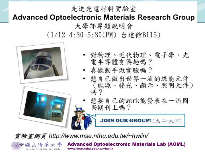
Advanced Optoelectronic Materials Lab (AOML) www.mse.nthu.edu.tw/~hwlin
Outline • Advanced Optoelectronic Materials Laboratory in NTHU, MSE • Small Molecule Organic Photovoltaics (OPV) and Organic Light Emission Devices (OLED) • Why small molecules? • Device structures and optical designs • Molecule structures and designs • Recent Progress • 大學部專題研究規劃 Advanced Optoelectronic Materials Lab (AOML) www.mse.nthu.edu.tw/~hwlin
I. Advanced Optoelectronic Materials Laboratory (AOML) Advanced Optoelectronic Materials Lab (AOML) www.mse.nthu.edu.tw/~hwlin
Brief History 2012 2011 2010 • Keep working and keep growing 2009 • Very high efficiency device (OPV, OLED,…) demonstrated • - 1 Group Leader • - 4 PhD Student • - 7 Master Student • Fabrication and measurement facilities move-in • - 1 Group Leader • - 1 PhD Student • - 5 Master Student • Lab established • - 1 Group Leader • - 2 Master Student Advanced Optoelectronic Materials Lab (AOML) www.mse.nthu.edu.tw/~hwlin
Facilities 2010 • Fabrication and measurement facilities move-in Advanced Optoelectronic Materials Lab (AOML) www.mse.nthu.edu.tw/~hwlin
Facilities (Fabrication) • Room 319, MSE building, NTHU • Vacuum evaporator integrated with N2 glove box • Sputter • Spin coater (one in N2 glove box and one in air) • Blade coating facilities • Hood • Temperature gradient sublimation system • Deionized water system • Microbalance • Humidity Cabinets • Dispenser, UV lamp for encapsulation 2010 • Fabrication and measurement facilities move-in Advanced Optoelectronic Materials Lab (AOML) www.mse.nthu.edu.tw/~hwlin
Facilities (Measurements) • Room 332-1, MSE building, NTHU • UV-Vis spectrometer with absorption/reflection option • Solar cell testing station(Solar simulator, Semiconductor parameter analyzer) • Photoresponse measurement system (Xe lamp, Monochromator, Current preamplifier, Lock-in amplifier with chopper, GPIB computer interface) • Multi-core CPU high-speed computer for multi-physics and quantum chemistry simulation • OLED testing station (Semiconductor parameter analyzer, Spectrophotometer with fiber collector, Probe station, Large area blue-enhanced Si-detector) • Time of flight measurement system(oscilloscope, high power Q-switch pulsed laser, 2nd and 3rd harmonic generation optics, cryostat, high voltage source) • Organic laser measurement system • Absolute quantum yield measurement system • Time resolved PL / EL measurement system • Transient absorption spectroscopy • Transient photocurrent / photovoltage spcetroscopy 2010 • Fabrication and measurement facilities move-in Advanced Optoelectronic Materials Lab (AOML) www.mse.nthu.edu.tw/~hwlin
Main Theme Solution Processed SMOLED Small Molecule OSC (SMOSC) Inverted OSC Host materials for PHOLED Organic Solar Cell OLED Solution Processed SMOSC Crosslinkable HTL for OLED Microcavity OSC Os(II) PHOLED AOML Exciton & Carrier Dynamics in OSC Organic Thin-Film Laser Device physics of DSSC Organic Thin-Film Sensor Novel OE Device Photophysics Light outcoupling of OLED Organic Photodetector Plasmonic effect Organic-Inorganic Hybrid Device Advanced Optoelectronic Materials Lab (AOML) www.mse.nthu.edu.tw/~hwlin
Group Members Organic Solar Cell OLED AOML Novel OE Device Photophysics Advanced Optoelectronic Materials Lab (AOML) www.mse.nthu.edu.tw/~hwlin
II. Organic Small Molecule Solar Cells Advanced Optoelectronic Materials Lab (AOML) www.mse.nthu.edu.tw/~hwlin
Why Small Molecules for OSCs? Polymer OSC Small Molecule OSC • Defined molecule structure • Purification by vacuum sublimation • Very good batch-to-batch reproduction • More advanced layer structures • Ready for tandem configuration • Vacuum & solution process are all possible Advanced Optoelectronic Materials Lab (AOML) www.mse.nthu.edu.tw/~hwlin
Fundamental Research of Small Molecule Solar Active Thin Films Intermolecular Charge Transport Space-charge-limited-current and time-of-flight technique Molecular structure and stacking Electronic structure Morphology Photophysics Electronic transitions Photoinduced electron transfer Exicton dynamics Geminate & Non-geminate recombination HOMO Morphology Interpenetration bulk heterojunction networks Surface topology Molecular self-assembly (crystallization, aggregation) Spectroscopy Spectroscopy Ellipsometry Absorption spectroscopy Time-resolved spectroscopy Photoresponse spectroscopy Impedance spectroscopy Advanced Optoelectronic Materials Lab (AOML) www.mse.nthu.edu.tw/~hwlin
Simulation Fully Optical and Electrical Simulation Optical Simulation Electrical Simulation • Rigorous classical electrodynamics • General layered media (wavelength dependent • optical constants, anisotropic) • Both optically “thin” and “thick” layers • Full angle, full polarization and full spectrum • Exciton diffusion dynamics and carrier transport behavior • Exciton diffusion meet with criteria of boundary • conditions in organic neat films • Carrier transports with recombination • Current density in target spectra can be modeled Advanced Optoelectronic Materials Lab (AOML) www.mse.nthu.edu.tw/~hwlin
D-π-A molecule η = 3.8 % ChemChomm 47, 7872 (2011) Advanced Optoelectronic Materials Lab (AOML) www.mse.nthu.edu.tw/~hwlin
A-A-D-A-A molecules η = 3.7 % Org. Lett. 13, 4962 (2011) Advanced Optoelectronic Materials Lab (AOML) www.mse.nthu.edu.tw/~hwlin
D-A-A molecules (DTDCTB) Advanced Optoelectronic Materials Lab (AOML) www.mse.nthu.edu.tw/~hwlin
D-A-A molecules (DTDCTB) Voc: 0.79 V Jsc: 14.68 mA/cm2 FF: 0.50 η = 5.8 % JACS ASAP (2011) Advanced Optoelectronic Materials Lab (AOML) www.mse.nthu.edu.tw/~hwlin
D-A-A molecules (DTDCTP) DTDCTB DTDCTP Voc: 0.95 V Jsc: 12.1 mA/cm2 FF: 0.56 Voc: 0.79 V Jsc: 14.68 mA/cm2 FF: 0.50 η = 5.8 % η = 6.4 % Submitted (2011) Advanced Optoelectronic Materials Lab (AOML) www.mse.nthu.edu.tw/~hwlin
On-going Progress New donor with optimized HOMO/LUMO level Optimization of device structure η > 7 % Solution processed SMOSCs η ~ 7 % η > 5 % Flexible SMOSCs ITO-free SMOSCs η ~ 5 % η > 5 % Inverted SMOSCs η > 5 % Advanced Optoelectronic Materials Lab (AOML) www.mse.nthu.edu.tw/~hwlin
Best Cell Efficiency Advanced Optoelectronic Materials Lab (AOML) www.mse.nthu.edu.tw/~hwlin
III. Small molecular Organic light emitting diode Advanced Optoelectronic Materials Lab (AOML) www.mse.nthu.edu.tw/~hwlin
Visible Light • Visible Light is electromagnetic radiation of a wavelength that is visible to the human eye Advanced Optoelectronic Materials Lab (AOML) www.mse.nthu.edu.tw/~hwlin
Blue OLED Device FIrPic Advanced Optoelectronic Materials Lab (AOML) www.mse.nthu.edu.tw/~hwlin
Green OLED Device Advanced Optoelectronic Materials Lab (AOML) www.mse.nthu.edu.tw/~hwlin
Red OLED Device Advanced Optoelectronic Materials Lab (AOML) www.mse.nthu.edu.tw/~hwlin
Binary White OLED 100 nits ~ 1000 nits CIE = (0.33, 0.34) (0.33 , 0.34) Advanced Optoelectronic Materials Lab (AOML) www.mse.nthu.edu.tw/~hwlin
Trinary White OLED CIE Values lie on CCT Curve! Color rendering index (CRI) achieve 79 Ir(mppy)3 Ayu-1195 FIrpic Advanced Optoelectronic Materials Lab (AOML) www.mse.nthu.edu.tw/~hwlin
High CRI White OLED CRI enhances up to 84! Os(bpftz)2(dppb) Ayu-1195 FIrpic Advanced Optoelectronic Materials Lab (AOML) www.mse.nthu.edu.tw/~hwlin
Color Tuning OLED Color temperature 4600~1600 K Advanced Optoelectronic Materials Lab (AOML) www.mse.nthu.edu.tw/~hwlin
OLEDs In Near Future Advanced Optoelectronic Materials Lab (AOML) www.mse.nthu.edu.tw/~hwlin
IV. 大學部專題研究 Advanced Optoelectronic Materials Lab (AOML) www.mse.nthu.edu.tw/~hwlin
Some Successful Examples • 專題成果刊登於Organic Electronics (IF = 3.998) • 專題成果刊登於Organic Letters (IF = 5.250) • 專題成果本月準備投稿 • 專題成果獲國科會大專學生專題研究補助 Advanced Optoelectronic Materials Lab (AOML) www.mse.nthu.edu.tw/~hwlin
Schedule • 一月底~二月 • 開始專題研究 • 認識材料基本光學性質(n, k),利用Silicon n, k計算反射率(Matlab基礎實習),並認識反射頻譜儀及基本光纖式光譜儀助教:陳昶文 • 三月 • 觀摩有機薄膜沈積,量測有機薄膜附著在Si基板之反射率推算薄膜厚度與光學性質(Matlab進階實習)助教:林偉桀、黃正宇 • 四月 • 量測OLED與OPV基本特性(光電量測儀器實習)助教:范嘉展、呂誌偉 • 五月 • 量測儀器電腦控制與記錄(Labview)基礎實習助教:范嘉展 • 六月 • 光電元件基板準備與固態薄膜沈積助教:陳奕宏、張容浩 • 七月以後 • 開始前瞻研究! Advanced Optoelectronic Materials Lab (AOML) www.mse.nthu.edu.tw/~hwlin
What You Should Participate? • Group Meeting (weekly) • 專題生基本研究進度 Meeting (Bi-weekly, with T.A.) • 實驗室公共事務 (值週生) • After having you own project: Join one of the sub-group meeting, literature report in group meeting Advanced Optoelectronic Materials Lab (AOML) www.mse.nthu.edu.tw/~hwlin
What You Can Gain from This Project? What you can learn: • 基礎材料光電特性量測 • 基礎科學工程軟體使用與程式撰寫 • 有機光電薄膜與元件製程 If you stick with us long enough… • 屬於你自己的最先進有機能源元件研究題目 • 自己動手做世界上從來沒有人做過的實驗、成為世界上發現某自然界奧妙的第一人 • 發表你的work在國際上重要的期刊,開始在世界舞台上嶄露頭角! Advanced Optoelectronic Materials Lab (AOML) www.mse.nthu.edu.tw/~hwlin
Some New Projects • Functional Organic Nano Structure Advanced Optoelectronic Materials Lab (AOML) www.mse.nthu.edu.tw/~hwlin
Some New Projects • Alternative Fabrication Technique Advanced Optoelectronic Materials Lab (AOML) www.mse.nthu.edu.tw/~hwlin
THANK YOU FOR YOUR ATTENTION Advanced Optoelectronic Materials Lab (AOML) www.mse.nthu.edu.tw/~hwlin