Download
1 / 44
440 likes | 592 Views
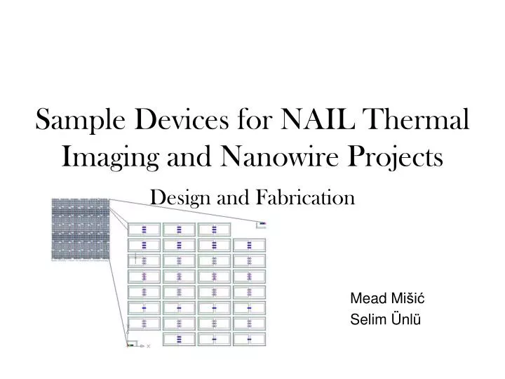
Sample Devices for NAIL Thermal Imaging and Nanowire Projects. Design and Fabrication Mead Mi šić Selim Ünlü. Outline. The NAIL and Nanowire Projects NAIL Microscopy and Applications Nanowire Research Objectives Sample Requirements Sample Design and Mask Fabrication

E N D
Sample Devices for NAIL Thermal Imaging and Nanowire Projects Design and Fabrication Mead Mišić Selim Ünlü
Outline • The NAIL and Nanowire Projects • NAIL Microscopy and Applications • Nanowire Research Objectives • Sample Requirements • Sample Design and Mask Fabrication • Process of Sample Device Manufacturing • Conclusion • Questions Boston University
Problem with the imaging of the Si ICs Metal layer on top of the ICs often make imaging from the substrate an easier option Boston University
Conventional Optical Microscopy • Refraction reduces sinθa by a factor of n, so maximum θa=θc • Total internal reflection θc = sin-1(1/n) • Resolution Diminished Boston University
NAIL Microscopy • Using a silicon lens as a coupler • Maximum θa = π/2 • Reflection loss at interfaces is minimized. • Evanescent wave coupling between the NAIL and substrate • Resolution Improved Boston University
NAIL Thermal Imaging Tests Imaging test with aluminum wires With NAIL Without NAIL Boston University
NAIL Thermal Imaging Resolution No actual real device-like sample imaged yet Boston University
Drawing of the previous nanowire sample The Nanowire Project The goal is to research the conductivity of polymer nanowires for possible integrated sensing applications Nanowire Conductor Metal Au Metal Au Silicon Substrate Boston University
Drawing of the proposed device for high throughput measurements of the transport properties of conducting polymer nanowires. Nanowire Sample Proposal Nanowire Conductor Metal Metal Oxide Oxide n+ or p+ n+ or p+ Boston University
Sample Device Requirements • NAIL Requirements • Emission lines ranging from 0.8um - 5.0um • Width of the spaces between the emission lines ranging from 0.8um - 5.0um • To generate a sufficient amount of emission • Nanowire Project Requirements • Space between implant areas varying • Conducting areas to be flat (implanted) • Samples to be manufactured on silicon substrate • Samples to be manufactured using the same masks Boston University
Design Constraints and Decisions • 4 inch platform • Large metal contact areas • P-type pre-doped wafers • All ion implants to be n-type • Leakage prevention (isolation implant or etch) • Leave room for error Boston University
The Wafer Mask Layout The picture shows the layout of the devices in CAD using all 5 masks. The masks were manufactured at EPFL in Switzerland. Boston University
A Die Layout Boston University
Basic Device Dimensions 3500um The dimensions indicated are identical in all the devices. 1600um 1500um 400um 100um 1500 um Boston University
NAIL – Periodic Devices • Each Device contains 3 implant sections like the one above, with each section containing two samples • Samples consist of lines and spaces of equal thicknesses • The thicknesses are: 0.8, 1.0, 1.2, 1.5, 2.0, 5.0 um Metal Line Isolation Implant Line Metal Line Boston University
NAIL – Aperiodic Devices • Each device contains 3 implant sections like the one above with each section containing 2 samples • Samples consist of lines of constant width and variable spacing. • The spacing widths are: 0.8, 1.0, 1.2, 1.5, 2.0, 5.0um Metal Line Isolation Implant Line Metal Line Boston University
NAIL - Variable Width Device • Device to be used for NAIL Qualification • 100um x 100um metal to implant contact • Line thicknesses: 0.8,0.9,1.0,1.2,1.5,2.0,3.0 um • Spacing between the lines 10um constant Metal Line Isolation Implant Line Metal Line Boston University
NAIL – Parallel Devices • There are two separate Parallel Devices • 0.8-1.2 um parallel device • 1.5-3.0 um parallel device • Each device contains 3 samples, and each sample has lines of variable width and constant spacing in between Metal Line Isolation Implant Line Metal Line Boston University
Nanowire Devices • Similar size and dimensions as in NAIL devices • Large metal contacts for easy activation • Implant areas a varying space apart for nanowire lines to be drawn Boston University
Nanowire Devices • There are 2 different nanowire devices with 3 samples on each device. • Separation distances between the implant areas are: 1, 2, 3, 5, 10, and 20um Boston University
Sample Device Fabrication • 5 Masks manufactured, 4 being used • 4 inch wafer platform • 5 p-type lightly doped wafers • Implants used all n-type • Using BU ECE semiconductor manufacturing lab equipment, ion implanters from Implant Sciences, and potentially other tools. Boston University
Fabrication – Silicon Wafers • Lightly P-doped Silicon Wafers • 5 Pieces • One side polished Si <100> 22 ohm*cm Boron (p-) doped wafer Boston University
Phase 1 – Photoresist Application • PR Shipley S1813 Photoresist • 4000 RPM for 30 Seconds • Uniform 1.5um thickness • Development Photoresist S1813, Thickness=1.5um Si <100> 22 ohm*cm Boron (p-) doped wafer Boston University
Phase 1 - Mask 1 Exposure • UV Exposure using S. Microtek • Expose at 8mW for 12sec Mask 1 Si <100> 22 ohm*cm Boron (p-) doped wafer Boston University
Phase 1 - Etching into Silicon • Etch 700nm into Silicon • Isolation Trench and Aligner Markers • Easier Navigation while Processing Si <100> 22 ohm*cm Boron (p-) doped wafer Boston University
Phase 1 – PR Removal and Cleaning • PR Removal using Acetone, Methanol, and DI Water • Particle Removal using RIE Asher Si <100> 22 ohm*cm Boron (p-) doped wafer Boston University
Phase 2 – P+_130keV Simulation Boston University
Phase 2 - Photoresist Application • PR S1813 Photoresist • 5000 RPM for 60 Seconds • Uniform 1.0um thickness • Development Photoresist S1813, Thickness=1.0um Si <100> 22 ohm*cm Boron (p-) doped wafer Boston University
Phase 2 - Mask 3 Exposure • UV Exposure using S. Microtek • Expose at 8mW for 12sec Mask 3 Si <100> 22 ohm*cm Boron (p-) doped wafer Boston University
Phase 2 - P+_130keV Implant • Phosphorus Ion Implant at 130keV with 1e15 ions/cm^2 and 7 degree θ angle done at Implant Sciences P+ Si <100> 22 ohm*cm B- doped wafer Boston University
Phase 2 - PR Removal and Cleaning • PR Removal using Acetone, Methanol, and DI Water • Using HTEA recipe on Fusion Asher P+ Si <100> 22 ohm*cm Boron (p-) doped wafer Boston University
Phase 2 – Ion Implant Anneal • 3 minute anneal at 1050C • Longer anneal expands the implanted area and activates it fully • This implant will create a pn-junction preventing any leakage between the metal contacts. P+ Si <100> 22 ohm*cm B- doped wafer Boston University
Phase 3 – As+_30keV Simulation Boston University
Phase 3 – Photoresist Application • PR S1813 Photoresist • 6000 RPM for 90 Seconds • Uniform sub-1.0um thickness • Development Photoresist S1813, Thickness <1.0um P+ Si <100> 22 ohm*cm Boron (p-) doped wafer Boston University
Phase 3 - Mask 4 Exposure • UV Exposure using S. Microtek • Expose at 8mW for 12sec Mask 3 Mask 4 P+ Si <100> 22 ohm*cm Boron (p-) doped wafer Boston University
Phase 3 - As+_30keV Implant • Arsenic Ion Implant at 30keV with 1e15 ions/cm^2 and 7 degree θ angle done at Implant Sciences P+ As+ Si <100> 22 ohm*cm B- doped wafer Boston University
Phase 3 – PR Removal and Cleaning • PR Removal using Acetone, Methanol, and DI Water • Using Fusion Asher HTEA recipe P+ As+ Si <100> 22 ohm*cm Boron (p-) doped wafer Boston University
Phase 3 – Ion Implant Anneal • 30 second anneal at 1100C • Short anneal time prevents the implanted area from expanding P+ As+ Si <100> 22 ohm*cm Boron (p-) doped wafer Boston University
Phase 4 – Photoresist Application • PR S1813 Photoresist • 4000 RPM for 30 Seconds • Uniform 1.5um thickness • Development Photoresist S1813, Thickness=1.5um P+ As+ Si <100> 22 ohm*cm Boron (p-) doped wafer Boston University
Phase 4 - Mask 5 Exposure • UV Exposure using S. Microtek • Expose at 8mW for 12sec Mask 3 Mask 5 P+ As+ Si <100> 22 ohm*cm Boron (p-) doped wafer Boston University
Phase 4 – Aluminum Sputtering Aluminum deposition via evaporation P+ As+ Boston University
Phase 4 – Aluminum Liftoff and PR Removal • Al Liftoff to remove the extra aluminum • PR removal using Acetone, Methanol and DI Water P+ As+ Boston University
Conclusion • To provide samples for NAIL thermal imaging and Nanowire projects • NAIL: Provide various 0.8um-5.0um features for imaging in various configurations • Nanowire: Provide samples with implanted areas connected to large metal contacts • A sufficient amount of samples • Leave a foundation for simpler future sample device manufacturing Boston University
Questions? Boston University