Download
1 / 27
270 likes | 463 Views
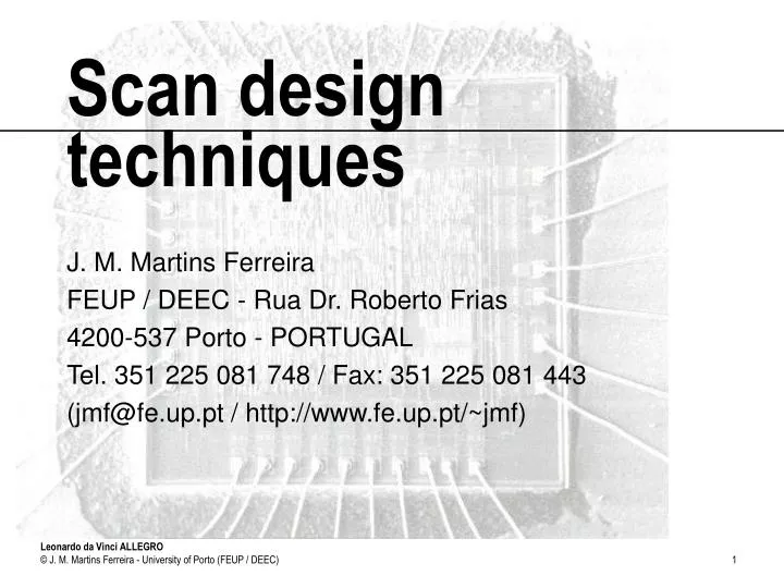
Scan design techniques. J. M. Martins Ferreira FEUP / DEEC - Rua Dr. Roberto Frias 4200-537 Porto - PORTUGAL Tel. 351 225 081 748 / Fax: 351 225 081 443 (jmf@fe.up.pt / http://www.fe.up.pt/~jmf). Objectives. To introduce the basic concepts in design for test

E N D
Scan design techniques J. M. Martins Ferreira FEUP / DEEC - Rua Dr. Roberto Frias 4200-537 Porto - PORTUGAL Tel. 351 225 081 748 / Fax: 351 225 081 443 (jmf@fe.up.pt / http://www.fe.up.pt/~jmf)
Objectives • To introduce the basic concepts in design for test • To prepare the introduction of the standard boundary-scan test architecture
Outline • Testability and test generation in sequential circuits • Testability improvement via ad hoc solutions • Structured approaches to design for testability
Test generation for sequential circuits • Direct application of the D-algorithm leads to the combinational circuit inputs and outputs, not necessarily to primary inputs or outputs
Combinational block A=1 Next state output 1 U?A X s@0 1 (1/0) 3 1 2 Circuit 7408 U?A 1 primary 3 output 2 F=1/0 0 0 U?A 7432 1 3 0 2 Next state 7408 output VCC_BAR U?A 1 0 7474 6 CL Q 3 CLK 1 1 5 2 CLK PR Q D 4 VCC_BAR U?A 1 0 7474 6 A CL Q 3 CLK 1 5 2 PR Q D fault-free 4 F CLK VCC_BAR X s@0 Test generation - step 3 The second clock cycle is applied with A=1 and guarantees fault detection, because the circuit is now brought to a state where fault activation and fault propagation are simultaneously possible.
The general case is however much more complex... • The D-algorithm does not necessarily lead to circuit primary inputs and outputs • Knowledge of the state transition diagram is required • It may happen that the fault affects the state transition diagram, in which case the required sequence at the circuit primary inputs becomes even harder to find
The case of Y s@0 • Test vector generation for a fault that affects the state transition diagram will help us to understand the problem
Q1,Q0=00 Q1,Q0=00 0 0,1 0 0 0,1 1 0 01 01 1 1 1 0 10 10 2 2 1 States 1 and 3 0 (Q0=1) are no 1 longer accessible 3 3 11 11 The case of Y s@0 (cont.) • Modification in the state transition diagram: Q1 Q0
Ad hoc testability improvements • Design rules or amendments to avoid or minimise test vector generation problems • Major drawbacks: • Not always reusable • Testability depends largely on the type of circuit
Some ad hoc testability rules • Split counters to avoid high numbers of clock cycles until the required output combination is achieved • Include reset and preset lines (synchronous or asynchronous) • Partition large circuits and add extra inputs and outputs for direct controllability and observability of internal nodes
Structured Design for Testability (DfT) • Structured DfT methodologies enable a simple way to drive the circuit to any given state in a fixed (and short) number of clock cycles • Does structured DfT have drawbacks? • Design rules (design styles) have to accepted • Additional silicon area, more pins and higher propagation delays… but is this an additional cost?
The scan design principle • The scan design principle consists of inserting a 2:1 multiplexer between the input of every D flip-flop and its driving logic
Scan design advantages (1) • Problem: Part of the combinational circuit inputs are not directly controllable, since they come from the D-FF outputs (these nodes define the present state of the circuit) • Solution: Scan flip-flops enable direct controllability of the D-FF outputs through a simple procedure with a fixed number of clock cycles
Better controllability through scan design (1) Example Take the circuit to state 110, starting from state 100 (intrusive)
Scan design advantages (2) • Problem: Part of the combinational circuit outputs are not directly observable, since they go to the D-FF inputs (these nodes define the circuit next state) • Solution: Scan flip-flops enable direct observability of the D-FF inputs through a simple procedure with a fixed number of clock cycles
Better observability through scan design (1) Example Observe the next state (eventually non-intrusive)
DfT: Eventually an overhead • The 2:1 muxs increase the propagation delay and require additional silicon area and pins, but will this increase cost? • How do we quantify the benefits of easier test vector generation and application? • Design freedom was traded for higher testability, but partial scan design might be a preferred intermediate solution