Download
1 / 15
200 likes | 445 Views
Graphene Flake Electrodes for Super Capacitor. Meng Jiao. Introduction of Super Capacitor. The fast development of electronics require new energy storage devices. 1. Smaller, lighter 2. High efficiency 3. Environmental friendly 4. Longer life 5. L ower cost.

E N D
Graphene Flake Electrodes for Super Capacitor Meng Jiao 5/5/2010
Introduction of Super Capacitor • The fast development of electronics require new energy storage devices. 1. Smaller, lighter 2. High efficiency 3. Environmental friendly 4. Longer life 5. Lower cost Your logo here
Possible solution: Super capacitor • 1. High energy density (unit: Wh/kg) Your logo here
Continued • 2. Efficiency comparison (Recharge) Data citied from: 1. http://en.wikipedia.org/wiki/Electric_car 2. John W. Stevens and Garth P. Corey, John W. Stevens and Garth P. Corey, (http://photovoltaics.sandia.gov/docs/PDF/batpapsteve.pdf ) Your logo here
continued • 3. Fast recharge • Ather advantages: 1. low coast 2. Longer life 3. Environmental friendly Your logo here
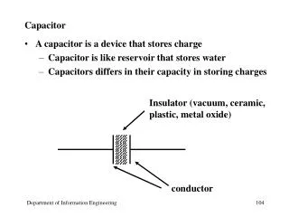
How it works Structure Scheme: Electrodes: Made from large surface area material such as active carbon. Ionic liquid: electrolyte Separator: Effective ion conductor. Your logo here
Electric Double Layer (EDL) • A model proposed by Helmholtz Your logo here
How This Model Works Assume no chemical reaction happen at electrode surface, then no charge transfer. Ions form a thin layer on electrode. Separation between them is determined by the radius of ions and the solvation shells. A video lecture about EDL: http://www.youtube.com/watch?v=2zhQM0IfTcI (Picture and material quote from http://www.cartage.org.lb/en/themes/sciences/Chemistry/Electrochemis/Electrochemical/ElectricalDouble/ElectricalDouble.htm) Your logo here
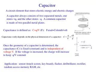
Large Capacitance • Capacitance: C • EDL provide a charge separation d in order of Å. As comparison the thinnest dielectric man can made is about 2 μm. • Then we need to do is choose electrode with large surface area Your logo here
The Electrode Currently in Use • Active carbon Surface area: 500 m2/gram Data and pic quoted from Wikipedia. http://en.wikipedia.org/wiki/Activated_carbon Your logo here
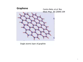
Graphene Surface area of Graphene: Single layer: 2500 m2/gram Double Lyaer: 1200 m2/gram (calculation are based on bond length 0.14nm) Picture quoted form wikipedia http://en.wikipedia.org/wiki/Graphene Your logo here
Electrode • The proposed electrode are achieved by two approaches with exactly the same idea. Maximize the Area. Your logo here
Approach 1 • Mix CNT with chemically prepared graphene flakes. (details of this process can be found in the paper J. Am. Chem. Soc., 1958, 80 (6), p 1339) • The purpose of adding CNT is to build a electronic conducting network. The graphenesuspended in the electrolyte to maximize the electrode surface area. They can pick up charges only when they in touch with the CNT network. Your logo here
Approach 2 • Graphenenanomesh + graphene flakes. Details about carbon nanomesh please see JingweiBai, et al. Graphenenanomesh, Nature Nanotech. 5, 190 (2010) • The electrodes are composed with layers of nanomashes, which allow the free flow of electrolyte. In between layers, graphene flakes present to provide separation between mesh layers and maximize the surface area. Your logo here
Reference • JingweiBai, et al. Graphenenanomesh, Nature Nanotech. 5, 190 (2010) • paper J. Am. Chem. Soc., 1958, 80 (6), p 1339 • http://en.wikipedia.org/wiki/Graphene • http://en.wikipedia.org/wiki/Activated_carbon • http://www.cartage.org.lb/en/themes/sciences/Chemistry/Electrochemis/Electrochemical/ElectricalDouble/ElectricalDouble.htm • http://www.youtube.com/watch?v=2zhQM0IfTcI • John W. Stevens and Garth P. Corey, John W. Stevens and Garth P. Corey, http://photovoltaics.sandia.gov/docs/PDF/batpapsteve.pdf • http://en.wikipedia.org/wiki/Electric_double-layer_capacitor Your logo here