Download
1 / 33
340 likes | 375 Views
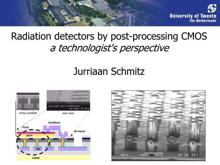
Radiation detectors by post-processing CMOS a technologist's perspective Jurriaan Schmitz. Outline. The semiconductor industry today The future, for industry and academia The concept of wafer post-processing Famous examples Recent successes Outlook. 10 4. 10 3. Cost per component.

E N D
Radiation detectors by post-processing CMOS a technologist's perspective Jurriaan Schmitz
Outline • The semiconductor industry today • The future, for industry and academia • The concept of wafer post-processing • Famous examples • Recent successes • Outlook
104 103 Cost per component 102 10 1 1 10 102 103 104 105 Number of components in an IC Source: www.intel.com
Source: www.intel.com Intel: Moore’s Law will outlive CMOS(Orczyk, Leuven, 2005)
Source: www.intel.com More performance… … at lower cost
The state of the art (1): CMOS • Nanometer precision • Sub-ppm materials purity IBM IBM IBM Intel
The state of the art (2): FLASH • 50-nm FLASH • Nanometer precision • Sub-ppm materials purity
The state of the art (3): DRAM • 58-nm DRAM technology Qimonda (Infineon) SAMSUNG • Nanometer precision • Sub-ppm materials purity
The Roadmap for Semiconductors The coming 10 years will bring: • Faster, cheaper transistors • Faster, cheaper memories • Lower power, faster communication • … again? • Already, the worldwide production of transistors exceeds that of rice grains
Is Moore’s Law a blessing? • It brought us into the Digital Age • It makes the semiconductor business (somewhat) predictable for economists • It creates a lot of employment … but there is little room for creativity! Transistors, transistors, transistors… Smaller, smaller, smaller…
But there is more! Source: ENIAC Industry & academia Industry Industry & academia
Traditional IC: Computing Data Storage Electrical Communication Possible extensions: High quality passives Wireless communication Optical communication Sensing and Actuating More than Moore: new functions What’s 15*2.2? Thirty-three How do we benefit from the present IC quality, and still add new functions?
The technological challenge How to combine electronics with sensors, actuators, optical components, …? • Hybrid (solder components together) • Pre-CMOS: Make component, then make CMOS on the same wafer • Intermediate: Mix the component and CMOS processes • … or post-CMOS: add components on top of a finished CMOS chip
MEMS-first monolithic integration Sandia 3-D accelerometer
Intermediate processing • mix MEMS and CMOS fabrication NIST gas sensor Kovalgin, J. Electrochem. Soc. 153 (9) H181
a. Chip fabrication Wafer post-processing b. Wafer dicing
a. Chip fabrication b. Post-processing c. Wafer dicing Wafer post-processing
Chip fabrication: standard, at any regular (CMOS) fab Post-processing: special,in a custom CR laboratory Wafer dicing, packaging: specialized work like MEMS packaging, e.g. Amkor, Boschman a. Chip fabrication b. Post-processing c. Wafer dicing Logistics
We do not interfere with the (CMOS) fab process We can buy good quality chips We can use any lab for this We must keep the CMOS intact We have to think the final stages through very carefully! a. Chip fabrication b. Post-processing c. Wafer dicing Pros and cons Flexible for R&D; potential for mass-scale manufacturing
Example: Liquid-Crystal-on-Silicon Cover glass Electrode Liquid crystal Reflector CMOS
Example: CMOS image sensor Incident light ~ 2 mm lens lens Quartz cover R/G/B filter R/G/B filter Image sensing chip Chip housing photodiode photodiode silicon
CMOS on top of CMOS? (3D integration) T ≤ 450 °C B. Rajendran et al., IEEE Trans. El. Dev. 54 (4) 707. A. W. Topol et al., IBM J. Res. & Dev. 50 (4/5) 491 • Technologically within reach! • Issues: • A cold dielectric • A high quality semiconductor • A killer application…
CMOS post-processing Careful treatment of the underlying CMOS: • Temperature ≤ 400 °C • Mild (or no) plasmas • Maintain the H balance in the MOSFET • Limited mechanical stress The CMOS properties must be unchanged:then the standard infrastructure can be used.
Low temperature ↔ high energy • Cool the substrate, heat up the surface Laser annealing Remote-plasma CVD T. Shimoda et al., Nature 440, 783-786 ICP source at MESA+ clean room
InGrid Beyond electronics: radiation imaging Traditional MWPC Particle Cathodeplanes Anodewires
InGrid: top performance! • Excellent energy resolution for a gaseous detector • 3-D track reconstruction • Fast, low power, low cost per channel • On-site data reduction / processing possible • See contribution by V. M. Blanco Carballo
The next step: other imagers Light imaging • Integrate an MCP • Semiconductor on a chip • 3D integration • X-ray imaging • HEP tracking • …… Scintillator on imager chip CEA-LETI IEDM 2006 Vallerga UC Berkeley Wyrsch et al.: Si SigmaDigitalXray
Conclusions What can we build on top of CMOS? • More electronics • Light projectors • CMOS imagers • Radiation imaging detectors There’s plenty of room at the top!
Thanks… My low-temperature coworkers: • Tom Aarnink, Victor Blanco Carballo, Arjen Boogaard, Ihor Brunets, Jisk Holleman, Alexey Kovalgin, Jiwu Lu, Joost Melai, Cora Salm, Sander Smits, Rob Wolters • Max Chefdeville, Harry van der Graaf, Marten Bosma, Jan Visschers, Jan Timmermans Our sponsors: • The Dutch Technology Foundation • NXP Research • Adixen/Alcatel • ASM International Our website: http://sc.ewi.utwente.nl
Postprocessing: further reading Jurriaan Schmitz, Nucl. Instr. Meth. A 576 (2007) 142. Our website: http://sc.ewi.utwente.nl