Download
1 / 136
1.36k likes | 1.43k Views
Learn about basic circuit concepts, capacitance, resistance estimations, MOS device capacitances, routing capacitance, analytic inverter delays, and VLSI design processes and flow. Discover the Y-chart design flow, stick diagrams, CMOS layers, design rules, layout diagrams, scaling of MOS circuits, and limitations of scaling.

E N D
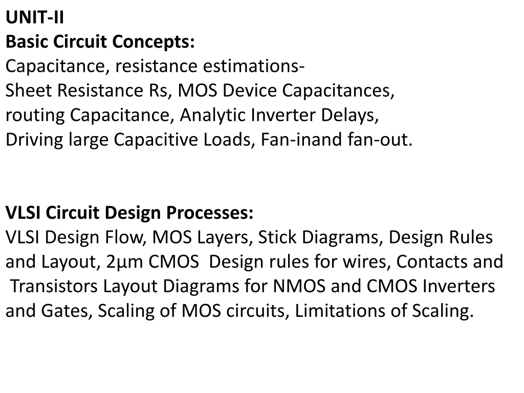
UNIT-II Basic Circuit Concepts: Capacitance, resistance estimations- Sheet Resistance Rs, MOS Device Capacitances, routing Capacitance, Analytic Inverter Delays, Driving large Capacitive Loads, Fan-inand fan-out. VLSI Circuit Design Processes: VLSI Design Flow, MOS Layers, Stick Diagrams, Design Rules and Layout, 2μm CMOS Design rules for wires, Contacts and Transistors Layout Diagrams for NMOS and CMOS Inverters and Gates, Scaling of MOS circuits, Limitations of Scaling.
MOS circuits are formed on four basic layers: • N-diffusion • P-diffusion • Polysilicon • Metal • These layers are isolated by one another by thick or • thin silicon dioxide insulating layers. • Thin oxide mask region includes n-diffusion / p-Diffusion and transistor channel.
VLSI DESIGN FLOW The Y-chart ( first introduced by D. Gajski ) is shown in below figure illustrates a design flow for most logic chips, using design activities on the three different axes (domains). Y chart of three major domains, they are: • Behavioral domain • Structural domain • Geometrical layout domain
Front-end design includes digital design using hardware description languages(HDLs), design verification through simulation and formal verification techniques, synthesis of digital designs to gates, and design for testability. Back-end design consists of CMOS library design and characterisation, physical design (floor-planning, placement and routing), design for manufacturability, packaging, test generation and fault simulation.
Stick diagram : • Stick diagrams may be used to convey layer information • through the use of a color code. Stick diagrams are a means of capturing topography and layer information using simple diagrams. Acts as an interface between symbolic circuit and the actual layout. A stick diagram is a cartoon of a layout.
Rules for drawing Stick Diagram Rule 1 : When two or more ‘sticks’ of the same type cross or touch each other that represents electrical contact.
Rule 2 : When two or more ‘sticks’ of different type cross or touch each other there is no electrical contact. (If electrical contact is needed we have to show the connection explicitly).
Rule 3: When a poly crosses diffusion it represents a transistor.
Rule 4 : In CMOS a demarcation line is drawn to avoid touching of p-diff with n-diff. All pMOS must lie on one side of the line and all nMOS will have to be on the other side.
CMOS NOR Gate : VDD A B Vout
CMOS NAND Gate : VDD Vout A B
Layout Design Rules The physical mask layout of any circuit to be manufactured using a particular process must conform to a set of geometric constraints or rules, which are generally called layout design rules. These rules usually specify the minimum allowable line widths for physical objects on-chip such as metal and polysilicon interconnects or diffusion areas, minimum feature dimensions, and minimum allowable separations between two such features.
The design rules are usually described in two ways : • Micron rules, in which the layout constraints such as minimum feature sizes and minimum allowable feature separations, are stated in terms of absolute dimensions in micrometers, or, • Lambda rules, which specify the layout constraints in terms of a single parameter (L) and, thus, allow linear, proportional scaling of all geometrical constraints.