Download
1 / 168
1.7k likes | 1.95k Views
Rapid Prototyping Using Field Programmable Devices. Allen C.-H. Wu Department of Computer Science Tsing Hua University Hsinchu, Taiwan 30043, ROC email: chunghaw@cs.nthu.edu.tw. Outline. Introduction to programmable logic devices and rapid prototyping.

E N D
Rapid Prototyping Using Field Programmable Devices Allen C.-H. Wu Department of Computer Science Tsing Hua University Hsinchu, Taiwan 30043, ROC email: chunghaw@cs.nthu.edu.tw
Outline • Introduction to programmable logic devices and rapid prototyping. • FPGA design technologies and applications. • Logic emulation. • Reconfigurable computing and systems.
Part I Introduction to Programmable Logic Devices and Rapid Prototyping
Programmable Logic Devices • SPLDs (simple PLDs). • CPLDs (complex PLDs). • FPGAs (field programmable gate arrays). • SPGAs (system-programmable gate arrays).
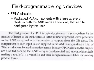
Programmable Interconnect Components • FPID: I-Cube. - Dynamic switching. - Communication switches, network routes. - 32-320 programmable I/O ports. - Up to 150 MHz clock frequency. • FPIC: Aptix. - 1024 programmable I/O ports.
SPLD • Universal designs. • Useable gates < 1,500 gates. • Speed is the main advantage. • 0.5um CMOS -> 3.5ns logic delays -> 200 MHz. • Market is shrinking 5-7% per year.
CPLD • Rising densities/performance and declining prices => become a good choice for many applications. • 100K gates today, 250K gates by 1998. • Low-density CPLD (32 macrocells/44 pins) -> 5ns logic delays, high-density CPLD (128 macrocells/100 pins) -> 7.5ns.
FPGA FPGA Antifuse- programmed SRAM- programmed EPROM- programmed Island Cellular Actel ACT1 & 2 Quicklogic’s pASIC Crosspoint’s CP20K Altera’s MAX AMD’s Mach Xilinx’s EPLD Xilinx LCA AT&T Orca Altera Flex Toshiba Plesser’s ERA Atmel’s CLi
Categories of FPGA’s • Block organized, SRAM based. • Channel organized, antifuse based. • SOP organized (each logic cell likes a PAL device), various programming techniques.
S S S S L L L S S S S L L L S S S S L L L S S S S Block organized, SRAM based
SRAM cell SRAM cell SRAM Programming Technology “1” -> “on” “0” -> “off” Pass transistor i1 i2 “1” -> o = i1 “0” -> o = i2 Mux o
SRAM Programming Technology • Advantages: - Reprogrammability. - Quality -> parts are fully tested at the factory. - Standard process technology. • Disadvantages: - Volatile -> FPGA must be reprogrammed each time when power is applied. - Need an external memory to store the program. - Large area (6 trs for 1 cell + 1 switch).
Antifuse Programming Technology Poly Dielectric Substrate Small antifuse area! Diffusion - Normally in high-Z state. - Can be fused to low impedance. - High-voltage melts dielectric causes link poly and diffusion.
EPROM/EEPROM Technology • EPROM can be reprogrammed, no need for external storage. • EPROM can not be re-programmed in circuit. • EEPROM can be re-programmed in circuit. • EEPROM consumes 2X more area as EPROM.
Logic array Registers I/Os Erasable PLD (EPLD) SOP-based PAL In, Out, bidirection Configured to D, T, JK, SR FFs. Programmable clock to each FF.
Programming the FPGA • Configuration. • Readback - design verification and debugging. • Security - a security-bit to prevent readback.
Advantages and Disadvantages of FPGA • Fast turnaround. • Low NRE (non-recurring engineering) changes. • Low risk. • Effective design verification. • low testing cost. • Chip size & cost. • Slow speed.
CPLD Vs. FPGA CPLD FPGA Interconnect style ContinuousSegmented Architecture and timing PredictableUnpredictable Software compile times ShortLong In-system performance FastModerate Power consumption HighModerate Applications addressed Combinational andRegistered registered logiclogic only Source: Altera
FPGA Selection Criteria • Density. • Speed. • Price. • Flexibility.
SPGA • Allow multiple building blocks. • Logic. • Memory. • Data path.
Applications Using SPGAs • Intellectual property (IP). • Communication & networking. • Graphical processing. • Embedded processing.
Designing with SPGAs • A team-based approach. • Understanding how to use SPGA system features will be the key to pulling the entire design into a single device.
CMOS PLD Market Share 31% 5% 3% 5% 24% 6% 11% 15% Source:dataquest
CMOS Logic Market 8% 14% 10% 30% 9% 29% Source:dataquest
FPGAs Growth Source: Integrated Circuit Engineering
CMOS Programmable-logic Market Source:dataquest
Rapid Prototyping • What? • Why? • How?
What is prototyping? • Basic components: FPGAs and FPICs. • Hardware : boards, boxes, and cabinets. • Software: methodologies and CAD tools.
Market survey Product development Production Product Development Cycle Customer acceptance
Pressures on Today’s Product Development • Time-to-market! • Design complexity!
Why Needs Prototyping? • Design verification. • Limited production. • Concurrent engineering.
Specification Functionality & requirements ? Final functionality & performance Final product Design Verification
Design Process Specification System-level design Simulation RTL design Fast prototyping Formal verification Logic-level design Logic emulation Physical-level design Final chips
Verification Alternatives System integration Modeling accuracy Prepare time Speed Event Driven Simulation High No Short Slow Cycle-Based Simulation Med. No Short Med. Behavioral Simulation Low No Short Med. Hardware Accelerated Sim Varies No Med. Med. Fast Breadboarding Med. Yes Long Very Fast Emulation or Prototyping Med. Yes Med. Very Fast
A Minute in the Life of a 100K Gates Design 1 --------- Actual hardware at 50MHz 10 -------- Logic emulator or prototype at 5MHz 100------- 2K-------- HW accelerator at 250M evals/sec 50K------- Cycle-based simulator at 1K insts/sec 120K----- Compiled-code logic simulator at 125MIPs 800K----- Event-driven logic simulator at 125 MIPs 1 Mon. 3 Mon. 1.5 Yr.
SW Integration Integration Code Design Design Build Design Fab Debug Debug Debug Development with Prototyping HW CHIP
System Integration & SW Debug Code Design Design HW Integration & Debug Build Final Integration Chip debug Design Fab Development with Prototyping SW HW CHIP
How to Develop a Prototyping using FPDs • Custom-designed prototyping board. • Logic-emulation systems. • Field-programmable printed-circuit-boards.
Part II FPGA Design Technologies and Applications
FPGAs • What? - Programmable logic + programmable routing = FPGAs. • Why? - Zero NREs, easy bug fixes, and short time-to-market. • How?
Comparison of Different Design Technologies Custom Std Cells Gate Arrays FPGAs Design time Long Short Short Short Fabrication Long Long Short None Chip area Small Med. Large Very large Design cost High Med. Low Very low Unit cost Low Low Med. High Design cycle Long Med. Short Very short
Emerging FPGA-based Applications • Low-volume production. • Urgent time-to-market competition. • Rapid prototyping. • Logic emulation. • Custom-computing hardware. • Reconfigurable computing.
Design Considerations • Target architecture. • Fixed logic and routing resources. • Fixed I/O pins. • Slow signal delays.
An HDL-based Design Flow HDL design specification RTL synthesis Verification (Simulation) Logic synthesis Physical synthesis FPGAs
Design Specification • HDLs - VHDL and Verilog. • Why needs an HDL-based design methodology? • Target Applications. • Coding Styles. • Design representation. • Design entry.
Why Needs an HDL-based Design Methodology Design complexity Then Now Schematic capture HDL design specification Component mapping & may be some logic optimization Synthesis Place & route Place & route Layouts Layouts SW : assembly language => high-level language
Target Applications and Layout Architectures • Datapath dominated designs : DSPs and processors. • Control dominated designs: controllers and communication chips. • Mixed type of designs. • Bit-sliced stacks. • Standard cells. • Macro-cell-based. • FPGAs.
HDL Coding Styles Vs. Design Quality Ideas? HDL spec1 HDL spec2 HDL spec3 Synthesis system Design3 Design2 Design1
Coding Styles and Design Representation • Hierarchical style • Structural style • Random style • FSMD • Behavioral level • Logic level • Gate level module MUX2(o,i1,i2,sel); output[1:4] o; input[1:4] i1,i2; input sel; assign o[1] = ((sel&i1[1])|(~sel&i2[1])); assign o[2] = ((sel&i1[2])|(~sel&i2[2])); assign o[3] = ((sel&i1[3])|(~sel&i2[3])); assign o[4] = ((sel&i1[4])|(~sel&i2[4])); endmodule module MUX2(o,i1,i2,sel); output[1:4] o; input[1:4] i1,i2; input sel; reg[1:4] o; always case(sel) 1’b0: o = i1; 1’b1: o = i2; endcase endmodule