Download
1 / 74
740 likes | 865 Views
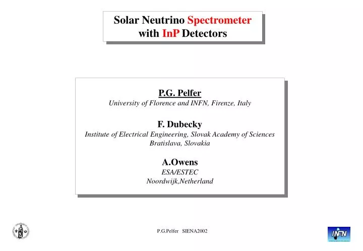
P.G.Pelfer SIENA2002. Solar Neutrino Spectrometer with InP Detectors. P.G. Pelfer University of Florence and INFN, Firenze, Italy F. Dubecky Institute of Electrical Engineering, Slovak Academy of Sciences Bratislava, Slovakia A.Owens ESA/ESTEC Noordwijk,Netherland.

E N D
P.G.Pelfer SIENA2002 Solar Neutrino Spectrometer with InP Detectors P.G. Pelfer University of Florence and INFN, Firenze, Italy F. Dubecky Institute of Electrical Engineering, Slovak Academy of Sciences Bratislava, Slovakia A.Owens ESA/ESTEC Noordwijk,Netherland
Why InP Solar Neutrino Experiment ? Semi Insulting InP Material base material for: Hard X-Ray Detectors Fast Electronics and Optoelectronics InP Spectrometer, the Smallest, Real Time, Lower Energy pp Solar Neutrino Spectrometer The Solar Neutrino Spectrometer from/for R&D on InP X-Ray Detectors ? P.G.Pelfer , SIENA2002
Requirements for Hard X-Ray Detectors of the NewGeneration • Room temperature (RT) operation • Portability • Fast reaction rate • Universal detection ability • Good detection parameters: CCE, FWHM, DE • Radiation hardness • Well established material technology • Well established device technology (10 m) • FE Electronics and Optoelectronics integration on the Detector • LOW COST RT OPERATION: EG > 1.2 eV POLARISATION EFFECT: EG < 2.5 eV HIGH ENERGY RESOLUTION: EG small HIGH STOPPING POWER:Z > 30 HIGH CARRIER MOBILITY: > 2000 cm2/Vs CANDIDATES CdTe, HgI2, GaAs, InP P.G.Pelfer , SIENA2002
BASIC KNOWLEDGE • Solar Neutrino Physics • X-ray astronomy • X-ray physics • MEDICINE • Digital X-ray radiology (stomatology, mammography, ...) • Positron emission tomography • Dosimetry • NONDESTRUCTIVE ON-LINE PROCESS CONTROL • Material defectoscopy • MONITORING • Environmental control • Radioactive waste management • Metrology (testing of radioactive sources, spectrometry...) • NATIONAL SECURITY • Contraband inspections: cargo control • Detection of drugs and plastic explosives • Cultural heritage study P.G.Pelfer SIENA2002 DETECTOR APPLICATIONS
Present InP Material and Detector Technology SemiInsulating InP Wafer 6” diameter, 1 mm thick Basic Component of Neutrino Spectrometer Pad Detectors P.G.Pelfer SIENA2002
Neutrino from the Sun Chlorine Homestake e + 37Cl 37Ar + e- Gallium SAGE, Gallex, GNO e + 71Ga 71Ge + e- Water Kamioka, SuperK x + e- x + e- (ES) D2O SNO x + e- x + e- (ES) e + d p + p + e- (CC) x + d n + p + e- (NC) P.G.Pelfer , SIENA2002
P.G.Pelfer , SIENA2002 Requirements for Indium Solar Neutrino Spectrometer 1. Indium incorporated into the detector 2. Energy resolution ∆E/E of the order of 25% at 600 keV. Important for spectrometry as well as background reduction. 3. Time resolution of the order of 100 ns for ~ 100 keV radiations. 4. Position resolution ∆V/V 10-7 at a reasonable cost. Very important for background reduction 5. Good energy resolution for low energy radiations ( ~ 50 keV ) 6. Made with materials of high radiactive purity
P.G.Pelfer , SIENA2002 Neutrino Detection by In Target 1/2= 4.76 sec 7/2+ 612.81 keV e 9/2+ 1 3/2+ 497.33 keV 115In (95.7%) 1/2=6x1014 y - 2 1/2+ 0 115Sn E e(E - 118 keV ) + 115 Sn* Delay = 4.76 sec 115Sn* 115Sn + e-(88 112 keV)/1(115.6 keV) + 2(497.33 keV)
The Neutrino Tag a - e delay = 10 sec ( e/1 + 2 ) coincidence b - ( e/1 + 2) in prompt coincidence ( gate 100 ns ) c - ( e + e) in spatial coincidence in a microcell ( few mm3 ) d - 1 contained in a “ 1 cm3 cell “ surrounding primary microcell e - 2 shower trigger in at least two “ 1 cm3 cell “ f - 2containedina macrocell ( more than 27 “ 1 cm3 cell “ ) surrounding primary microcell g - E( e/1 ) = 50-200 keV h - E( 2 ) = 450-750 keV i- E(1 + 2 ) = 500-750 keV P.G.Pelfer SIMC XII July 2002, Smolenice Castle
1 cm3 cell 106 InP “1 cm3 cell” “ delayed event “ in a 27 cm3macrocell 1 neutrino event once a day for 1011 background events Calorimeter Module 3 4 5 " prompt event “ in a “1 cm3 cell” 2 2 1 6 1 3 4 5 9 8 7 time 2 1 6 e 9 8 7 10 s P.G.Pelfer , SIENA2002 Solar Neutrino Event inInP Detector
FULL NEUTRINO SPECTROMETER Spectrometer Building Block Nmodules 125 Spectrometer Module 100 mm 200 mm Pad Detectors Vmicrocell 1 mm3 Nmicrocell /cm3 1000 P.G.Pelfer , SIENA2002
Be (862) d * [SNU per 20 keV] pp pep (1442) P.G.Pelfer , SIENA2002 Be(384) spectrum of In (*10 ) E [keV] e 115 -11 Expected Electron Energy Spectrum from In Solar Neutrino Experiment
SI InP Material and Detector Technology Producer: JAPAN ENERGY Co., Japan Growth Technique: LEC High-Temperature Wafer Annealing Resistivity (300 K):4.9x107 cm Hall Mobility (300K):4410 cm2/Vs Fe Content:2x1015 cm-3 Orientation:<100> Final Wafer Thickness:~200 m Original BUFFERS realisedusing ion implantation in backside (PATENTED) Symmetrical circular contact configuration, 2mm , using both-sided photolithography Final metallisation: TiPtAu on top and AuGeNi on backside Surface passivation by Silicon Nitride P.G.Pelfer , SIENA2002
P.G.Pelfer , SIENA2002 InP Detector Test Setup 3.142 mm2 x 200 m
Energy Resolution vs Shaping Time and Spectral Response in InP Laboratory Measurements E=2.4 keV at 5.9 keV : 8.5 keV at 59.54 keV P.G.Pelfer , SIENA2002
P.G.Pelfer , SIENA2002 Linearity and Resolution vs X Ray Energy in InP Laboratory Measurements
HASYLAB X-1, BESSY-II WLS beamlines. Energy range 10 keV to 100 keV Beamline set-up Beam profile ~20 20 mm2, E/DE > 104 slits detector To mono/ focusing optics Beam pipe XY stage Optical bench P.G.Pelfer , SIENA2002 Synchrotron Radiation Measurements
Pulse Height Spectra inInP HASYLAB Measurements P.G.Pelfer , SIENA2002
P.G.Pelfer , SIENA2002 InP Derectors Linearity and Energy Resolution in the Measurements at HASYLAB
The detectors spatial response measured at HASYLAB using a 50 50 m2, 15 keV X-ray beam. bond wire contact P.G.Pelfer , SIENA2002 InP Spatial Distributions Count rate Peak centroid Resolving power
P.G.Pelfer , SIENA2002 InP Detector BESSY-II Measurements: Detection Efficiency vs Energy and Thickness Depletion depth derived from C/V measurements = 170 m Efficiency measured relative to a calibrated Ge(HP) detector Fitted depth from efficiency measurements = (191 40) m d= Aeoer/C WLS beamline
P.G.Pelfer , SIENA2002 InP Spectra Laboratory Cryogenic Measurements T=-170oC T=-60oC ST=10ms ST=2ms DE=2.4 keV at 5.9 keV : 8.5 keV at 59.54 keV DE=0.9 keV at 5.9 keV : 2.5 keV at 59.54 keV
Summary and Discussion Present Radiation Detectors based on BulkSI InP Fe doped have very good Detection Parameters for the X ray Detection from HASYLAB SR Facilty FWHM from 2.5 KeV at 5.9 KeV to 5.5 KeV at 100 KeV DE 10% at 100 KeV for 200 m thick Detector due to Better Material from Japan Energy and to Improved Interface Technology Some Problems for Detector Polarisation Detectors performance good for Solar Neutrino Spectrometer Optimisation is our next research goal P.G.Pelfer , SIENA2002
InP and In-Liquid Scintillator pp Solar Neutrino Detector InP DETECTROR In-Liquid Scintillator DETECTOR P.G.Pelfer , SIENA2002
Detectors tested E@5.9keV Area thickness E@5.9keV Area thickness Si 245 eV 0.9 mm2, 500mm CdZnTe 450 eV 3.1 mm2, 2500mm GaAs 470 eV 0.9 mm2, 40mm HgI2 600 eV 7.0 mm2, 500mm InP 2.5 keV 3.1 mm2, 180mm TlBr 900 eV 3.1 mm2, 800mm Bottom line: Si energy resolution degraded by a factor of 6 for a proton fluence of 8 x 10¹⁰ protons cm-2 (=60 krad), whereas InP degraded by only 20% for fluence of 1.6 x 10¹¹ protons cm-2 (however the initial resolution was much worse). P.G.Pelfer , SIENA2002 Radiation Damage Studies by 10 MeV Proton Beam Tests carried out at the accelerator facility of the Department of Chemistry, University of Helsinki, The incident beam energy was 10 MeV. Irradiations were carried out at room temperature and unbiased.
P.G.Pelfer , SIENA2002 Radiation Damage Studies. Energy Resolution vs Proton Fluence
ACKNOWLEDGEMENTS Authors are grateful to: Slovak Academy of Sciences Slovak Grant Agency and Slovak Ministry of Economy, European Spatial Agency, Istituto Nazionale di Fisica Nucleare, University of Florence P.G.Pelfer , SIENA2002
P.G.Pelfer , SIENA2002 Materials Requirements Detector Requirements Good energy resolution in the interval 50÷150 keV Large detector volume or thickness (mm) High ratio between peak to valley No high applied bias voltage Low dark current Short charge collection time High fabrication yield of good quality detectors Radiation Hardness Stability of detector in environmental conditions and ageing Relevant requirements depend from specific detector applications Bulk Material 1- , ee, hh :high mobility, long carrier lifetime and high product mobiliiy lifetime 2-material homogeneity in term of purity, stoichiometry, absence of structural defects. Highly uniform material critical for fabrication of thick X-Rays detectors. 3-high resistivity generally required (107cm) , high breakdown voltage, low dark current Epitaxial Materials not examined
Pad and Double Side Strip Detector Array PAMELA EMCal Si Microstrips Layers P.G.Pelfer , SIENA2002
Neutron Spectrography P.G.Pelfer , SIENA2002
Indium phosphide X-ray detectors • Possible room temperature operation • •High stopping power • Electron mobilities 3 times that of Si • Possible neutrino detection medium • Epitaxial and bulk growth available • Standard semiconductor processing
To mono/ focusing optics Synchrotron radiation measurements HASYLAB X-1 and BESSY-II WLS beamlines. Energy range 10 keV to 100 keV Beam profile ~20 20 mm2, E/DE > 104 Beamline set-up detector slits Beam pipe XY stage Optical bench
Science Payloads and Advanced Concepts Radiation damage studies: experimental Tests carried out at the accelerator facility of the Department of Chemistry, University of Helsinki using an IBA Cyclone 10/5, proton cyclotron, The incident beam energy was 10 MeV. Irradiations were carried out at room temperature and unbiased. Devices were tested using 55Fe, 109Cd and 241Am radioactive sources, with initial and final characterizations at HASYLAB Detectors tested E@5.9keV Area thickness E@5.9keV Area thickness Si 245 eV 0.9 mm2, 500mm CdZnTe 450 eV 3.1 mm2, 2500mm GaAs 470 eV 0.9 mm2, 40mm HgI2 600 eV 7.0 mm2, 500mm InP 2.5 keV 3.1 mm2, 180mm TlBr 900 eV 3.1 mm2, 800mm Bottom line: Si energy resolution degraded by a factor of 6 for a proton fluence of 8 x 10¹⁰ protons cm-2 (=60 krad), whereas InP degraded by only 20% for fluence of 1.6 x 10¹¹ protons cm-2 (120 krads Si equivalent), however the initial resolution was much worse.
Radiation damage studies: dose history Science Payloads and Advanced Concepts
X Rays Linear Scanner Linear array of 32 InP pixels Linear array of 32 InP pixel and FE electronics cooled with a Peltier cooler P.G.Pelfer , SIENA2002
P.G.Pelfer , SIENA2002 P.G.Pelfer , SIENA2002
Termonuclear Neutrino Sources from the Sun P.G.Pelfer , SIENA2002 P.G.Pelfer , SIENA2002