Download
1 / 21
300 likes | 619 Views
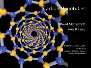
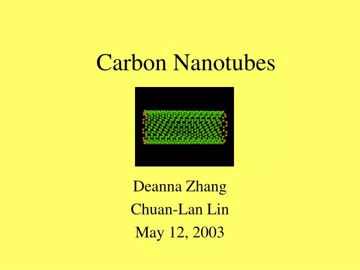
Carbon Nanotubes. Deanna Zhang Chuan-Lan Lin May 12, 2003. Overview. Introduction History Fabrication Application Summary. Introduction I: What is nanotube?. Responsible bond: Unit cell: honeycomb pattern Wrapping these patterns back on top of themselves and joining the edges

E N D
Carbon Nanotubes Deanna Zhang Chuan-Lan Lin May 12, 2003
Overview • Introduction • History • Fabrication • Application • Summary
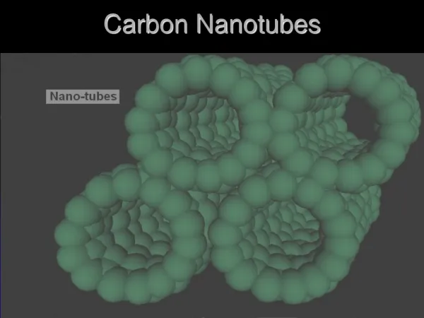
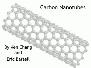
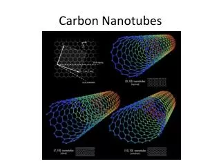
Introduction I:What is nanotube? • Responsible bond: • Unit cell: honeycomb pattern • Wrapping these patterns back on top • of themselves and joining the edges • Carbon nanotube
Introduction II:Single and Multi-wall nanotube • Single wall nanotube: • SWNT • single atomic layer wall, diameter of 1-5 nm • excellent mechanical property • hot topic now • Multi wall nanotube: • MWNT • Inner diameter: 1.5 – 15 nm • Outer diameter: 2.5 – 30 nm • ~50 layers • containing more structure defects (http://www.lbl.gov)
Introduction III:The Electrical Properties of nanotube • Can be either Metal or semiconductor • Controlled by Rolling Direction Ch (rolling vector)= na + mb (unit vector) Rule: = integer metallic non-integer semiconductor • Electrical Conductivity • Four Point Probe Method to determine sheet resistance and conductivity
Introduction IV:The Other Properties of Nanotube • Mechanical: • Young’s Modulus ~ 1TPa (SWNT), 1.25 TPa (MWNT) • (Steel: 230 GPa) • Density ~ 1.3 g/cm^3 • Thermal: • Conductivity: 2000W/m.K ( copper: 400W/m.K) • High Aspect Ratio: Length ~1µm, Diameter ~ 1nm to 50nm
History IBuckyball ( ) • The discovery of nanotubes comes from Buckyball • The discovery of Buckyball is by accident, from Radio-astronomy • Around 1970s (http://www.slb.com )
Fabrication of Carbon Nanotubes • Laser Ablation or Pulsed Laser Vaporization • Carbon Arc or Arc Discharge • Chemical Vapor Deposition (CVD) • High pressure (HiPCO)
Fabrication ILaser Ablation • Target: 1 at.% each of Ni and Co uniformly mixed with graphite • 500 m Torr Ar flowing at 50 sccm • In the oven at 1473 K • Nd:YAG Pulse laser at 60Hz • PUREST but yield is very small (~0.4 gram/hour) • Developed by NASA JSC Group based on Rice University facility
Fabrication IICarbon Arc or Arc Discharge • The first available method • Electric arc vaporizes an carbon anode containing the catalysts • (Ni and Co) • He: 500 Torr, Current: 100 amp and 35 volts • Chamber is cooled by water • Nanotube takes place at the wall inside the chamber • Developed by the group at the University of Monpellier, France
Fabrication IIIChemical Vapor Deposition (CVD) • Idea: prepattern the substrate with a catalyst and to grow nanotubes onto these by CVD • The key step : deposit the catalyst at predefined locations • Advantage: SELECTIVE GROWTH: we can grow nanotube at the place we expect • First developed by Xie group in China in 1996 • Use hydrocarbons as source
Fabrication III:Steps of CVD • Deposit photoresist • Expose resist • Deposit catalyst • Etch resist • CVD growth of Carbon Nanotube on catalyst
Fabrication IVHiPCO • Single wall nanotube in gas phase (1200C, 10 atm) • CO+CO C+ catalyst: (25 mTorr) • Flow high pressure carbon monoxide past catalyst particles at high temperatures • Can now produce largely single-walled nanotubes in kilogram quantities • Purification steps are unnecessarydue to use CO instead of hydrocarbons • (P. Nikolaev et al.)
Application • Transistor • Field Effect transistor • Single electron transistor • SPM Tips • Field Emission Display Device • More Possible Applications
Nanotube transistor • Field Effect transistor • Similar to MOSFET • Formation of P-type • Annealing or doping with K to form N-type • Use both N and P to make CMOS type circuits
SPM Tips • Tips of Scanning Probe Microscopes are usually cantilevers or metal wires but seldom survive a tip crash • Nanotubes: large aspect-ratio, well-defined end, far more resistant A nanotube was directly grown by CVD on a cantilever (From J. Hafner et al, Nature 398, 761 (1999))
Field Emission Display Device • Take advantage of the properties of high current containing and high aspect ratio • Useful as the electron source for Flat Panel Display with lower power consuming and high voltage circuit is unneeded • Samsung has shown the prototype of 9” full color display with 576 X 242 pixels • The first nanotube flat screen TV is expected to be manufactured by the end of 2003 The Samsung 4.5” full-color nanotube display (Anode) (Cathode) Schematic structure of nanotube flat panel display. (Choi et al.)
More Possible Applications • Nanotube sensors (Kong et al.): • The electrical conductivities of SWNT change dramatically when they expose to gaseous molecules • Hydrogen storage (Heben et al.): • 5~10 wt% hydrogen storage density at room temperature for SWNT • Light Elements (Saito et al.): • Electrons from nanotube bombard a phosphor-coated surface to produce light • 2 times brighter, 8000h lifetime, can be used for giant outdoors displays • Memory device (Fuhrer et al.): Capable to store single electronic charge • High mobility
Summary and Future work • Carbon Nanotubes have unique properties • Unique properties lead to fabrication of different devices. • Improvements of current fabrication of carbon nanotubes needed to make available commercial products. • The totally new world constructed by nanotube is close. • Little knowledge about growth mechanism