Download

1 / 30
310 likes | 603 Views
Biased PN junction Schottky diode. p. p. n. n. E. Reverse biased PN junction. Maximum electric field is located at x = 0. Reverse biased PN junction energy diagram. Voltage-dependent capacitor. p. n. p. n. Voltage-dependent capacitor.

E N D
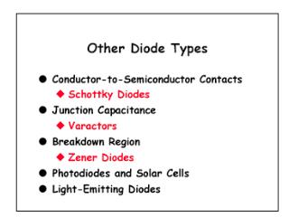
Biased PN junction Schottky diode
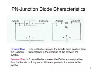
p p n n E Reverse biased PN junction
Maximum electric field is located at x = 0
p n Voltage-dependent capacitor
Example 5.5 Consider a gallium arsenide PN junction at room temperature. Determine the junction capacitance with a reverse bias voltage of 5 V.
Example 5.5 Consider a gallium arsenide PN junction at room temperature. Determine the junction capacitance with a reverse bias voltage of 5 V.
Forward biased PN junction n p - +
p n - E + Basic model – thermal equilibrium Thermal equilibrium implies Fermi energies are the same. Energy
Schottky barrier junctionEnergy levels before joining n Why?
Schottky barrier junctionThermal equilibrium n Energy - electrons depart leaving a region of ions – Fermi energies lineup Depletion width
n Schottky barrier junctionForward bias conditions Energy
Example 5.7 A silicon PN junction is forward biased at room temperature. Determine the voltage that is required to induce a particular diode current.