Download
1 / 18
200 likes | 481 Views
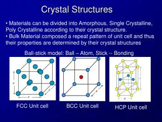
CRYSTAL STRUCTURES. LECTURE 5 (18 slides). z = up. x. y. Constructing an FCC crystal lattice. Note how the FCC is justifiably called cubic close-packed (CCP). y. x. y. x. Homework 5: A base 2-D close-packed square lattice can be found

E N D
CRYSTAL STRUCTURES LECTURE 5 (18 slides) Prof. Dave Smith
z =up x y Constructing an FCC crystal lattice Note how the FCC is justifiably called cubic close-packed (CCP). Prof. Dave Smith
y x y x Homework 5: A base 2-D close-packed square lattice can be found in the both the SC and FCC lattices. The 3-D extension differs, Resulting in a close-packed cubic lattice for FCC but a much less Dense SC layout. BCC is also not close-packed. Can you find, in any plane of the BCC lattice, a 2D close-packed structure? Discuss the (111) plane in this regard. What is the plane that looks closest to the one below? z =up Prof. Dave Smith
First layer Second layer Third layer Note: certain planes clearly show HCP patterns. HOME: what plane is this? Building an FCC lattice in an obvious way Prof. Dave Smith
Diamond and Zincblende Lattices 8-atom unit cell made from FCC 4-atom unit cell by putting another atom at a/4+b/4+c/4 from each FCC atom FCC Zincblende lattice has different species in FCC sublattices: e.g. InP, GaAs Prof. Dave Smith
BCC FCC Analyzing the diamond lattice Note: 4 bonds helps explain that C forms a diamond lattice structure Conclusion: the octant shown is an incomplete BCC lattice pattern. Use this in one of the HW’s Regarding packing fraction Prof. Dave Smith
Basic FCC lattice of Ga FCC lattice for As As Ga Our favorite nine III-V binary semiconductors form zincblende lattices Prof. Dave Smith
Hexagonal Close Packing Again, thanks to some popsicle sticks, some Elmer’s glue and a bunch of Marbles from Michael’s Arts and Crafts Store, a digital camera and Photoshop software HCP starting plane – builds up, but at each plane, one can choose different sites for the triad – as shown above Prof. Dave Smith
HCP and FCC contain HCP-type planes Hexagonal Close-Packed Cubic (FCC) Close-Packed Top view Open (seen from above) all layers Closed within 3 layers In fact, these lattice types have the same packing fraction. Prof. Dave Smith
Crystalline Element Lattice Types VII III IV V VI II HCP has 12 nearest neighbors diamond lattices BCC has 8 nearest neighbors Reference: http://www.uis.edu/~trammel/sci/unit_cells/sld30.htm Prof. Dave Smith
Assigned Problems 5-8. Streetman and Banerjee 6) 1.4 7) 1.7 8) 1.10 9) 1.14 Prof. Dave Smith
CRYSTAL GROWTH Prof. Dave Smith
Czolchraski Crystal Growth Method seed 12” diameter by 1 meter Si boule Made by pulling seed from Si melt Ref: S&B Figs. 1.10,1.11 Prof. Dave Smith
Epitaxial Growth Methods Start with suitably oriented crystal substrate – grow layers of identical (homoepitaxy) or different material (heteroepitaxy) maintaining lattice type, orientation and lattice constant. • LPE (Liquid Phase Epitaxy)– precipitation from liquid phase • onto substrate, controlled by time and temperature • VPE (Vapor Phase Epitaxy) – fast gas flow velocity over heated • substrates; surface reaction of compounds releases desired atoms • MBE (Molecular Beam Epitaxy) – for monolayer-level control • of stoichiometry – beams of elements to be deposited Reference: Mandatory reading (hand out): E. D. Jungbluth, “Crystal Growth Methods Shape Communications Lasers,” Laser Focus World, vol. 29, pp. 61-72 (Feb., 1993). Prof. Dave Smith
Epitaxial Growth Technologies LPE MBE VPE Reference: Mandatory reading (will hand out): E. D. Jungbluth, “Crystal Growth Methods Shape Communications Lasers,” Laser Focus World, vol. 29, pp. 61-72 (Feb., 1993). Prof. Dave Smith
2-D Lithography and etching at these stages Epitaxial Growth Methods 2” dia wafer cassette InP-based laser substrate Reference: G. P. Agrawal Reference: E. D. Jungbluth, ibid. Prof. Dave Smith
A superlattice of MBE-Grown Layers Alternating layers of GaAs (dark) and AlAs (light) with 4-monolayer periodicity: SUPERLATTICE CB VB Ref: S&B Fig. 1.16 Prof. Dave Smith
Assignment 10. Read. E. D. Jungbluth, “Crystal Growth Methods Shape Communications Lasers,” Laser Focus World, vol. 29, pp. 61-72 (Feb., 1993). a) What is an acceptable substrate defect density? b) How would you hook up a DC battery to make Jungbluth’s Fig 1’s device lase? How would you convert it into a detector instead? c) Compare substrate heating techniques in the cases of LPE, VPE and MBE. d) Several different bandgap-engineered devices types are mentioned and they are more suitable for some techniques than others. Name one type suitable for each fab method and why is that method preferred? E.g.: use the figure right bottom. Prof. Dave Smith