Download
1 / 16
170 likes | 428 Views
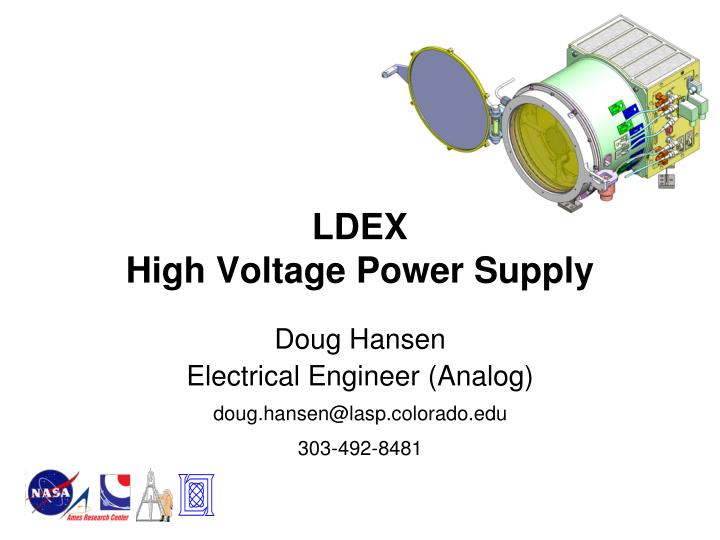
LDEX High Voltage Power Supply. Doug Hansen Electrical Engineer (Analog) doug.hansen@lasp.colorado.edu 303-492-8481. HVPS Driving Requirements and Capabilities HVPS Block Diagram Simulations of Key Subcircuits High Voltage Layout Methodology EMI Mitigation Current Status Future Plans.

E N D
LDEXHigh Voltage Power Supply Doug Hansen Electrical Engineer (Analog) doug.hansen@lasp.colorado.edu 303-492-8481
HVPS Driving Requirements and Capabilities HVPS Block Diagram Simulations of Key Subcircuits High Voltage Layout Methodology EMI Mitigation Current Status Future Plans Outline
HVPS Driving Requirements Output voltages supplied to the instrument (at the loads listed): Nom.Voltage @ Max. Load Flat Grid -1650 VDC 10 μADC MCP (Front) -700 VDC to -1100 VDC 200 μADC (adjustable in 25 V nom. steps) MCP (Back) -200 VDC -200 μADC Hemispherical Grid -200 VDC 1 μADC (switchable to +20 VDC) Solar Wind Screen -200 VDC 5 μADC
HVPS Driving Requirements Ripple allocations to the high voltage supplies: Requirement (max.)Est. Capability Flat Grid 200 mVrms 40 mVpp MCP (Front) 200 mVrms 40 mVpp MCP (Back) 50 mVrms 5 mVpp Hemispherical Grid 15 mVrms 5 mVpp Solar Wind Screen 200 mVrms 40 mVpp (Requirements do not consider benefit from synchronized sampling.)
HVPS Driving Requirements Additional allocations to the high voltage supplies: • Initial error plus temperature sensitivity of output voltages = ± 5.0 % (over full operating temperature range) Est. Capability = ± 1.8 % • Overshoot and transient change in MCP voltages due to dust impacts, turn-on or turn-off = 10 V (max.) Est. Capability = 0.5 V
H-Bridge Simulation TRANSFORMER PRIMARY CURRENT TRANSFORMER PRIMARY VOLTAGE
Voltage Multiplier Simulation UNREGULATED -400 VDC @ 10 uA INSTR. LOAD UNREGULATED -1400 VDC @ 200 uA INSTR. LOAD UNREGULATED -1800 VDC @ 10 uA INSTR. LOAD
Linear Regulator Simulation TURN-ON AND TURN-OFF TRANSIENT OF MCP/FRONT SUPPLY
Linear Regulator Simulation OVERSHOOT DURING MCP/FRONT SUPPLY TURN-ON TRANSIENT (APPX. ZERO)
Linear Regulator Simulation TRANSIENT RESPONSE OF MCP/FRONT SUPPLY DURING 40 us, 1.0E9 e- DUST IMPACT
Linear Regulator Simulation TRANSIENT RESPONSE OF MCP/FRONT SUPPLY DURING TURN-ON AND TURN-OFF OF MCP/BACK SUPPLY
High Voltage Layout Guidelines Layout will be based on NASA/TP-2006-214133, Design Guide For Space and results of internal peer reviews: • High voltage subcircuits will be isolated and potted. • Creepage fields will be limited to < 30 V/mil. • Electrostatic shielding will be provided around high voltage region in order to reduce dV/dt coupling to low voltage region. • Interconnection between high voltage and low voltage regions protected with diode clamps. • Low voltage region will be conformally coated. • All traces will have moderate radii at corners.
EMI Mitigation • Power switching frequency is 10x higher than front-end passband (where amplifier response is -30 dB). • Power switching is synchronized with front end ADC sampling. • Switching edges are slowed as much as possible. • Power transformer is a fully enclosed ferrite pot core. • Standard switching power supply layout guidelines will be used.
Current Status • Board requirements are defined and tracked in DOORS. • EM circuit design finished. • Peer review and one internal design review completed. • Responses provided for all peer review action items (that requested closure before the PDR). • EM layout ready to begin.
Future Plans • Complete layout and fabrication of EM card. • Evaluate EM card performance. • Complete simulations of a voltage multiplier that minimizes the number of unique capacitor part numbers.