Download
1 / 13
350 likes | 1.1k Views
Ionic Bonding: ex) alkali halide (NaCl) Each Na (atomic

E N D
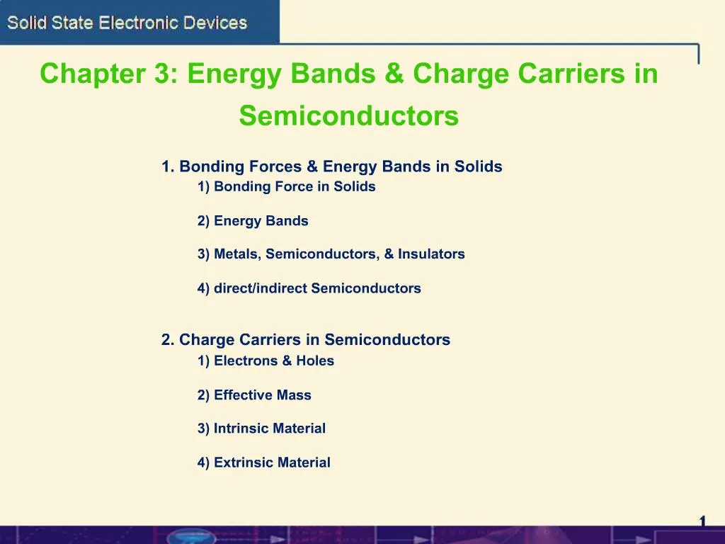
1. Chapter 3: Energy Bands & Charge Carriers in Semiconductors
2. Ionic Bonding: ex) alkali halide (NaCl)
Each Na (atomic #=11; [Ne]3s1) atom gives up its outer 3s electron to a Cl atom, so that Na atom is made up of Na+ positive ions with electronic structure of Ne(1s22s22p6).
Each Cl(atomic #=17; [Ne]3s23p5) atom receives an electron from a Na atom, so that Cl atom is made up of Cl- negative ions with electronic structure of Ar ([Ne]3s23p6)
Coulomb forces exerted between a Na+ & 6 Cl- balanced with repulsive forces
The ions have the closed-shell configurations of Ne and Ar ? no free electrons ? NaCl is a good insulator
1. Bonding Forces & Energy Bands in Solids
3. 1. Bonding Forces & Energy Bands in Solids
4. When 2 Si atoms are brought together:
Linear combinations of atomic orbitals (LCAO) for two-electron wave functions (?1, ?2) of atoms leads to 2 distinct �normal� modes: a higher energy anti-bonding (anti-symmetric) orbital, and a lower energy bonding (symmetric) orbital (Pauli�s exclusion principle)
For bonding state: an electron in the region between the two nuclei is attracted by two nuclei ? V(r) is lowered in this region ? electron probability density is higher in this region than for anti-bonding state ? It is the lowering of E of bonding state that causes cohesion of crystal 1. Bonding Forces & Energy Bands in Solids
5. When N Si atoms (1s:2N, 2s:2N, 2p:6N, 3s:2N, 3p:2N electrons) are brought together to form a solid:
As interatomic spacing decreases, the energy levels split into bands, beginning with valence (n=3) shell (sp3 hybridization) ? 3s & 3p bands grow and merge into a single band (8N states) ? As distance between atoms approaches the equilibrium interatomic spacing, this band splits into 2 bands separated by energy gap (Eg): upper band [conduction band; 4N states are empty(0K)], lower band [valence band; 4N states are completely filled with electrons (0K)].
6. Insulator:
Upper (conduction) band: empty (0K), lower (valence) band: completely filled with electrons (0K)
Eg > 5 eV (much greater in insulator than in semiconductors) ? # of electrons excited from valence band to conduction band due to the increases of temperature and light intensity ? 0 ? current ? 0 because no charge transport can take place
Semiconductor:
Upper (conduction) band: empty (0K), lower (valence) band: completely filled with electrons (0K)
Eg = 0.6-1.1 eV ? # of electrons excited from valence band to conduction band due to the increases of temperature and light intensity can be increased significantly ? current ? 0 because charge transport occurs
7. E (energy) - k (propagation constant; wave vector) relationship:
Free electron satisfies �k=<p>/h�
For e- within a periodic lattice( has a periodic potential function) :
energy gap Eg appears in E-k characteristics
11. Intrinsic Semiconductor: a perfect semiconductor with no impurities or lattice defects
VB is filled with electrons and CB is empty at 0K ? no charge carriers (insulator)
EHP Creation (bond model):
- If one of the Si valence electrons [gained enough E from higher T(=Eg; energy gap)] is broken away from its covalent bonds in the lattice such that it becomes free to move about in the lattice, a conduction electron is created and a broken bond (hole) is left behind. [valence electrons are excited thermally across Eg to CB (band model)]
12. Doping: the process to create carriers in semiconductors by purposely introducing impurities into the crystal
There are two types of doped semiconductors, n-type and p-type.
Extrinsic semiconductors: the materials that have a characteristic of n0 ? p0 ? ni when they are doped
n-type semiconductors:
A �donor� impurity from column V (P, As, Sb; donor) introduces an donor energy level (Ed) near the bottom of CB Ec( within the band gap)
At 50K, all of the electrons in Ed (filled with electrons at 0K) are �donated� to CB
(e-: majority carrier, h+: minority carrier)
13. p-type semiconductor (e-: minority carrier, h+:majority carrier):
An �acceptor� impurity from column III (B, Al, Ga, In; acceptor) introduces an acceptor energy level (Ea) near the top of VB Ev( within the band gap)
At 50K, all of the energy states in Ea (empty at 0K) �accept� electrons from the VB, leaving behind holes in the VB.