Download
1 / 5
50 likes | 71 Views
This proposal outlines a bus organization scheme for efficient FPGA communication, utilizing LVDS chips and connections, DC-DC converters, and control lines. The solution aims to optimize space and reduce the number of required chips.

E N D
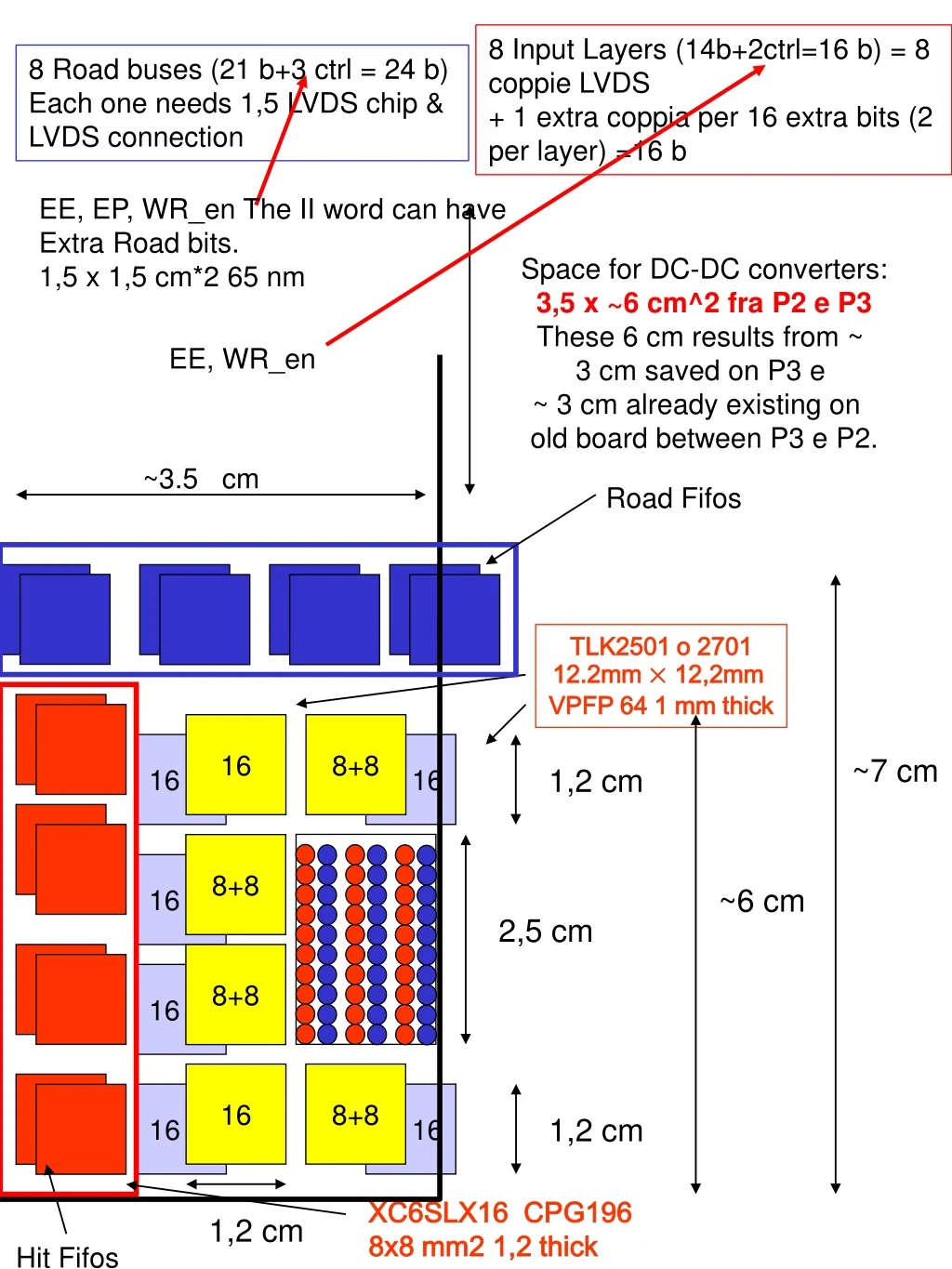
8 InputLayers (14b+2ctrl=16 b) = 8 coppie LVDS + 1 extra coppia per 16 extra bits (2 per layer) =16 b 8 Road buses (21 b+3 ctrl = 24 b) Each one needs 1,5 LVDS chip & LVDS connection EE, EP, WR_en The II word can have Extra Road bits. 1,5 x 1,5 cm*2 65 nm Space for DC-DC converters: 3,5 x ~6 cm^2 fra P2 e P3 These 6 cm results from ~ 3 cm saved on P3 e ~ 3 cm already existing on old board between P3 e P2. EE, WR_en ~3.5 cm Road Fifos TLK2501 o 2701 12.2mm × 12,2mm VPFP 64 1 mm thick 16 8+8 16 16 ~7 cm 1,2 cm 8+8 16 ~6 cm 2,5 cm 8+8 16 16 8+8 16 16 1,2 cm XC6SLX16 CPG196 8x8 mm2 1,2 thick 1,2 cm Hit Fifos
8 Road buses (25 b+8 ctrl = 33 bit)+ 3 control lines = 36 bits per bus. 2 words packet Each bus needs 1 LVDS chip & One LVDS connection NEW 8 InputLayers (15b+2ctrl=17 b) = 8 coppie LVDS EE, EP, WR_en Space for DC-DC converters: 3,5 x ~6 cm^2 fra P2 e P3 These 6 cm results from ~ 3 cm saved on P3 e ~ 3 cm already existing on old board between P3 e P2. EE, WR_en ~3.5 cm Road Fifos TLK2521 12.2mm × 12,2mm TQ 64 1,2 mm thick 18-18 18 ~7 cm 1,2 cm 18-18 16 ~6 cm 2,5 cm 18 18-18 18-18 18 1,2 cm XC6SLX16 CPG196 8x8 mm2 1,2 thick 1,2 cm Hit Fifos
Buses di uscita: • We have 20 bit addresses on AMchips, to address patterns that flow in 4-chip pipelines. • We add 3 bits in the LAMB GLUE to distinguish the 8 pipelines →from the LAMB GLUE we send out 23 bit road addresses. • We add extra 2 bits in the AMBoard to distinguish the 4 LAMBs →from the AMB we send out 25 bits • With the road address we send out also 8 bit bitmap • At the P3 we have 25+8 = 33 bits to transferred in two words, since they flow from the LAMB as 2 word-packets. Added to this we have3 controlbits:EE, EPandWR_EN. • We propose this organization into 2 words: 33+3=36 bits fit perfectly in a single chip (18 bits x 2 words = 36 bits). So we propose to use 1 chip/bus and put: • 1 chip/bus for a total of 8 buses transfer the bits produced by AMchips: • WR_Ex + 17 bits road first word • EEx, EPx + 8 bits bitmap + 8 bits road second word • The total number of needed chips is 8 instead of 12! • HIT BUSES: they fit perfectly in 1 chip/bus: • EEx, WR_ENx, 15 Hit bits = 17 bits.
Mixed solution to test both FPGA direct connection and TI transceivers – second word can be sent directly 8 Road buses (25 b+8 ctrl = 33 bit)+ 3 control lines = 36 bits per bus. 2 words packet Each bus needs 1 LVDS chip & One LVDS connection 8 InputLayers (15b+2ctrl=17 b) = 8 coppie LVDS Space for DC-DC converters: 3,5 x ~6 cm^2 fra P2 e P3 These 6 cm results from ~ 3 cm saved on P3 e ~ 3 cm already existing on old board between P3 e P2. EE, EP, WR_en EE, WR_en ~3.5 cm Road Fifos XC6SLX45T 4 GTPs XC6SLX45T 4 GTPs TLK2521 12.2mm × 12,2mm TQ 64 1,2 mm thick 18-18 18 ~7 cm 1,2 cm 18-18 16 ~6 cm 2,5 cm 18 18-18 18-18 18 1,2 cm XC6SLX16 CPG196 8x8 mm2 1,2 thick 1,2 cm Hit Fifos
Solution with GTXs (up to 6 GHz) + GTPs (up to 3 GHz) 8 Road buses (25 b+8 ctrl = 33 bit)+ 3 control lines = 36 bits per bus. 2 words packet Each bus needs 1 LVDS chip & One LVDS connection 8 InputLayers (15b+2ctrl=17 b) = 8 coppie LVDS Space for DC-DC converters: 3,5 x ~6 cm^2 fra P2 e P3 These 6 cm results from ~ 3 cm saved on P3 e ~ 3 cm already existing on old board between P3 e P2. EE, EP, WR_en EE, WR_en ~3.5 cm Road Fifos XC6VLX75T 8 GTXs 23x23 ~7 cm 1,2 cm + SY58602 SY58601 ~6 cm 2,5 cm XC6SLX45T 4 GTPs 15x15 XC6SLX45T 4 GTPs 15x15 1,2 cm 1,2 cm Hit Fifos