Download
1 / 34
400 likes | 1.02k Views
Series-Parallel Circuits. OBJECTIVES. Learn about the unique characteristics of series-parallel configurations and how to solve for the voltage, current, or power to any individual element or combination of elements.

E N D
OBJECTIVES • Learn about the unique characteristics of series-parallel configurations and how to solve for the voltage, current, or power to any individual element or combination of elements. • Become familiar with the voltage divider supply and the conditions needed to use it effectively. • Learn how to use a potentiometer to control the voltage across any given load.
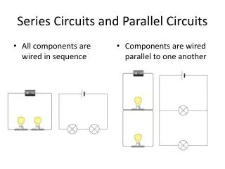
INTRODUCTION • A series-parallel configuration is one that is formed by a combination of series and parallel elements. • A complex configuration is one in which none of the elements are in series or parallel.
FIG. 7.1 Series-parallel dc network. SERIES-PARALLEL NETWORKS
FIG. 7.2 Introducing the reduce and return approach. REDUCE AND RETURN APPROACH
FIG. 7.3 Series-parallel network for Example 7.1. FIG. 7.4 Substituting the parallel equivalent resistance for resistors R2 and R3 in Fig. 7.3. REDUCE AND RETURN APPROACH
FIG. 7.5 Series-parallel network for Example 7.2. FIG. 7.6 Schematic representation of the network in Fig. 7.5 after substituting the equivalent resistance R for the parallel combination of R2and R3. REDUCE AND RETURN APPROACH
FIG. 7.7 Inserting an ammeter and a voltmeter to measure I4and V2, respectively. REDUCE AND RETURN APPROACH
BLOCK DIAGRAM APPROACH • Once the grouping of elements reveals the most direct approach, you can examine the impact of the individual components in each group. • This grouping of elements is called the block diagram approach
FIG. 7.8 Introducing the block diagram approach. FIG. 7.9 Block diagram format of Fig. 7.3. BLOCK DIAGRAM APPROACH
FIG. 7.11 Reduced equivalent of Fig. 7.10. FIG. 7.10 Example 7.3. BLOCK DIAGRAM APPROACH
FIG. 7.12 Example 7.4. BLOCK DIAGRAM APPROACH
FIG. 7.13 Reduced equivalent of Fig. 7.12. BLOCK DIAGRAM APPROACH
FIG. 7.15 Block diagram of Fig. 7.14. FIG. 7.14 Example 7.5. DESCRIPTIVE EXAMPLES
FIG. 7.16 Alternative block diagram for the first parallel branch in Fig. 7.14. DESCRIPTIVE EXAMPLES
FIG. 7.17 Example 7.6. DESCRIPTIVE EXAMPLES
FIG. 7.18 Block diagram for Fig. 7.17. FIG. 7.19 Reduced form of Fig. 7.17. DESCRIPTIVE EXAMPLES
FIG. 7.20 Example 7.7. DESCRIPTIVE EXAMPLES
FIG. 7.21 Network in Fig. 7.20 redrawn. DESCRIPTIVE EXAMPLES
FIG. 7.22 Example 7.8. DESCRIPTIVE EXAMPLES
FIG. 7.23 Network in Fig. 7.22 redrawn. DESCRIPTIVE EXAMPLES
FIG. 7.25 Determining VC for the network in Fig. 7.24. FIG. 7.24 Example 7.9. DESCRIPTIVE EXAMPLES
FIG. 7.26 Example 7.10. DESCRIPTIVE EXAMPLES
FIG. 7.27 Network in Fig. 7.26 redrawn. DESCRIPTIVE EXAMPLES
FIG. 7.28 An alternative approach to Example 7.10. DESCRIPTIVE EXAMPLES
FIG. 7.30 Network in Fig. 7.29 redrawn to better define a path toward the desired unknowns. FIG. 7.29 Example 7.11. DESCRIPTIVE EXAMPLES
FIG. 7.31 Complex network for Example 7.11. DESCRIPTIVE EXAMPLES
FIG. 7.32 Ladder network. LADDER NETWORKS • A three-section ladder network appears in Fig. 7.32. • The reason for the terminology is quite obvious for the repetitive structure. • Basically two approaches are used to solve networks of this type.
FIG. 7.33 Working back to the source to determine RT for the network in Fig. 7.32. LADDER NETWORKS
FIG. 7.34 Calculating RT and Is. FIG. 7.35 Working back toward I6. LADDER NETWORKS
FIG. 7.36 Calculating I6. LADDER NETWORKS
FIG. 7.37 An alternative approach for ladder networks. LADDER NETWORKS
FIG. 7.58 The dc bias levels of a transistor amplifier. APPLICATIONSElectronic Circuits
FIG. 7.59 Using PSpice to verify the results of Example 7.12. COMPUTER ANALYSISPSpice