Download
1 / 6
70 likes | 379 Views
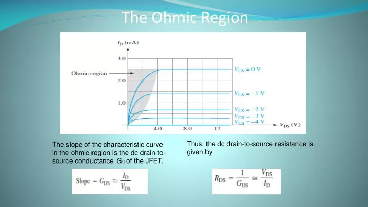
The Ohmic Region. Thus, the dc drain-to-source resistance is given by. The slope of the characteristic curve in the ohmic region is the dc drain-to-source conductance G DS of the JFET. The JFET as a Variable Resistance.

E N D
The Ohmic Region Thus, the dc drain-to-source resistance is given by The slope of the characteristic curve in the ohmic region is the dc drain-to-source conductance GDS of the JFET.
The JFET as a Variable Resistance • A JFET can be biased in either the active region or the ohmic region. • JFETs are often biased in the ohmic region for use as a voltage controlled • variable resistor. • The control voltage is VGS, and it determines the resistance by varying the Q-point.
The JFET as a Variable Resistance • To bias a JFET in the ohmic region, the dc load line must intersect the characteristic curve in the ohmic region. • Thus, to allows VDS to control RDS, the dc saturation current ID(sat), is set much less than IDSS so that the load line intersects most of the characteristic curves in the ohmic region.
The JFET as a Variable Resistance • Figure shows the operating region expanded with three Q-points shown (Q0, Q1, and Q2), depending on VGS. • As you move along the load line in the ohmic region, the value of RDS varies as the Q-point falls successively on curves with different slopes. • The Q-point is moved along the load line by varying
The JFET as a Variable Resistance • As this happens, the slope of each successive curve is less than the previous one. • A decrease in slope corresponds to less ID and more VDS, which implies an increase in RDS. • This change in resistance can be exploited in a number of applications where voltage control of a resistance is useful. • ***RDS is the DC drain to source resistance Q0: ID= 0.270mA, VDS=0.23V Q1: ID=0.250mA, VDS=0.33V Q2: ID=0.230mA, VDS=0.44V Q3: ID=0.210mA, VDS=0.56V