Download

1 / 44
1.85k likes | 5.25k Views
PEM Technologies BRINGING TECHNOLOGY TO THE INDUSTRY. IMPROVING YOUR WAVE SOLDERING. Igmar Grewar Technical Director PEM Technologies. Wave Soldering. Conveyor PCB transported over the wave . The 6 Basic Steps of Wave/Selective Soldering. Component preparation Insert components

E N D
PEMTechnologies BRINGING TECHNOLOGY TO THE INDUSTRY IMPROVING YOUR WAVE SOLDERING Igmar Grewar Technical Director PEM Technologies
Wave Soldering • Conveyor • PCB transported over the wave
The 6 Basic Steps of Wave/Selective Soldering • Component preparation • Insert components • Apply Flux • Preheat PCB • Soldering • Cool down
Preforming THT components • Cost saving • Higher production output • Quality
The effect of hole sizes • Hole size less than 1.5 times lead thickness – bend of slightly less than 90º • A dimple is formed on the lead for hole size more than 1.5 times lead thickness • Raised from PCB to allow for cleaning or heat dissipation
Selective Pallets • Stable support platform for PCB • Eliminate masking by hand • Eliminate glue dotting for SMD’s • Reduce solder defects such as skips and bridging • Pockets and channels promotes solder flow • Standardize conveyor width – reduce setup time • Multiple PCB’s on a pallet – higher throughput
The Wave Soldering Process Picture courtesy of Cobar/Balver Zinn
Fluxing Why do we need flux? • Prevents oxidation • Acts as a wetting agent Picture courtesy of Cobar/Balver Zinn
Fluxing – Wave Solder Two common types of fluxing methods in wave soldering: Foam fluxing Spray fluxing Pictures courtesy of Seho
Foam fluxing – Wave Solder • Flux control required • Ideal contact area = 20mm • Ideal flux stone pore size = 3um - 10um • Air pressure 2 - 3bar • Raise or lower the whole flux station to achieve the right contact • Never use a foam fluxer without an air knife • Not suitable for water based fluxes Picture courtesy of Seho
Flux Control (foam fluxer) Critical parameters: • Flux density (solid content) • Water content • Temperature • Contamination from PCB or compressed air • Replace flux in foam fluxers completely every 40 hours • Cleaning of foam pipe
Spray fluxing - Wave Solder • Single side PCB requires 100 Micro Gram per Cm2 of PCB surface (Check Flux Data Sheet) • PTH PCB’s will require 20% more • Check the spray pattern by wrapping a piece of photo sensitive fax paper around a bare PCB and let it run through the fluxer • Combination of airflow, flux flow, moving speed, distance of nozzle to PCB • Paper must be evenly gray from flux, not wet and certainly not dripping Picture courtesy of Seho
Advantages of Spray fluxing • Quantifiable application of the flux deposit (SPC) • No in-process QC of the flux • No thinner consumption • Direct application from can • Reduced flux consumption • No flux drippings over the preheat zone Picture courtesy of Seho
Conversion to Spray flux • The ‘Plug ’n Spray’ spray-fluxer • Stand alone fluxer Picture courtesy of Cobar/Balver Zinn Picture courtesy of Seho
Incorrect Flux Volume • Too little flux can cause soldering defects such as bridging and skips • Excessive flux can lead to solder balling and unwanted and uncured residue left on the PCB Picture courtesy of Bob Willis Picture courtesy of Cobar/Balver Zinn
Flux Types Alcohol based (100% VOC) • Long history of reliability & process know how • Modest in preheat requirements • Can be applied by spray or foam • High residue safety and wide process window • Hazardous & flammable material • Contributing to the "green-house" effect
Flux Types Low-VOC (40% water / 60% alcohol) • Modest in preheat requirements • Safer to the environment • Can be applied by spray or foam • High residue safety and wide process window
Flux Types Water based (100% VOC-free) • More soldering power • Environmentally safe • Non-flammable • Requires more preheat • Spray fluxing only • Some process adjustments required • Risk for corrosion if flux is not properly polymerized by the heat of the wave (flux under pallets, on topside or just too much flux applied)
Preheat Functions of Preheating • Evaporation of the solvent in the flux • Activating the flux • Minimizing the Delta T between the PCB and the solder wave Picture courtesy of Cobar/Balver Zinn
Preheat Types of Preheating Infra Red elements Quartz elements Forced Convection Pictures courtesy of Seho
The Preheat Profile • Preheat temperature is measured on the top side of the PCB • Typical max. preheat temperature Sn/Pb = 90ºC - 120ºC • Typical max. preheat temperature Pb-Free = 100ºC - 130ºC Picture courtesy of Cobar/Balver Zinn
Measuring Preheat Temperature Temperature Profiler / Thermocouples Adhesive Temperature Strips Infrared Thermometer Picture courtesy of TWS Automation Picture courtesy of www.tempstrips.com
Incorrect Preheat • Preheat too high or too long may break down the flux activation system and cause shorts / icicles • Preheat too low may cause problems such as skips or unwanted residues left on the PCB Picture courtesy of Cobar/Balver Zinn
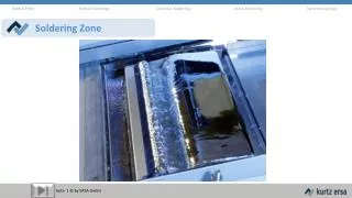
Soldering Phase • Wetting Phase • Wicking Phase • Drain Phase PCB ------ >> Wave Draining Wicking Wetting Picture courtesy of Cobar/Balver Zinn
Contact width 7º Soldering Phase • Nominal angle = 7º • Contact Width = 20 to 40mm wide for Delta Wave • Contact Width = 15mm wide for Chip Wave • Dwell time Tin/Lead = 3.5 sec @ 235ºC solder pot temperature • Dwell time Tin/Lead = 2.5 sec @ 250ºC solder pot temperature • Dwell time Pb-Free = 2 to 5 seconds @ 260-270ºC solder pot temperature, depending on the application • Conveyor speed = 0.8 – 1.5 m/min • Conveyor speed (m/min) = Contact width (cm) x Dwell time (sec) • Wave height = 1/3 – 2/3 of PCB thickness • High temperature glass plate is used to measure contact width and parallelism to the wave
Wave Nozzle Configuration Delta Nozzle • Standard Nozzle for through hole components • Fast moving solder moving in the opposite direction of PCB for wetting action • Small volume of solder moving along with the PCB for wicking action Picture courtesy of Bob Willis Picture courtesy of Seho
Wave Nozzle Configuration Chip Nozzle • Turbulent wave • Can be added in addition to the Delta Nozzle • High Kinetic Energy • Avoids shadowing Picture courtesy of Bob Willis Picture courtesy of Seho
Wave Nozzle Configuration Dual Wave • Turbulent chip wave combined with a slow moving horizontal wave overcomes the limitations of other wave types • Solution for overcoming the shadow effect on SMT components not aligned to the wave Picture courtesy of Seho Picture courtesy of Bob Willis Picture courtesy of Seho
Wave Nozzle Configuration Other Nozzles • For components requiring high wave pressure or high flow dynamics • For PCB’s with high thermal mass • To optimize contact time Pictures courtesy of Seho
Solder Alloy Lead Containing Alloy Sn/Pb • Contains Tin / Lead • Sn63/Pb37 • Melting point of 183ºC • Solder pot temperatures from 235 - 250ºC • Eutectic alloy – melts and solidifies at the same temperature • Low surface tension – good wetting • Low viscosity – great hole fill and top side fillet forming
Solder Alloy 4 Popular choices for Lead-Free • SAC (Tin/Silver/Copper) • SAC + X (Tin/Silver/Copper + X) • SnCu (Tin/Copper) • SnCuNi (Tin / Copper / Nickel) Your choice of alloy will be dependant on your specific requirements
Solder Alloy SAC • Tin / Silver / Copper • Typical: Sn96.5/Ag3.0/Cu0.5 • Melting point of 217 - 221ºC • Solder pot temperature 260ºC • High silver content • Solder joints looks different than Tin-Lead • Dull joints due to shrinkage
Solder Alloy SAC + X • Tin / Silver / Copper + X • X = Co, Fe, Bi, Si, Ti, Cr, Mn, Ni, Ge, and Zn • Typical: Sn98.3 Ag0.3 Cu0.7Bi0.7 • Melting point of 216 - 225ºC • Solder pot temperature 265ºC • Lower material costs vs higher silver SAC alloys • Performance and appearance similar to higher silver SAC alloys
Solder Alloy SnCu • Tin / Copper • Sn99.3/Cu0.7 • Melting point of 227ºC (Eutectic alloy) • No silver content - lowers alloy cost • Lower tendency to leach copper - less loss of conductive copper in tracks and pads • Poor fluidity at typical lead free temperatures • Poor through-hole filling and forming of solder bridges between components
Solder Alloy SnCuNi • Tin / Copper / Nickel • Sn99.25/Cu0.7/Ni0.05 • Melting point of 227ºC • Eutectic alloy – free of shrinkage • Solder pot temperatures from 265ºC • Does not contain silver - running costs are low • Small addition of nickel in to the SnCu alloy improves fluidity • Good fluidity – less bridges and better hole –filling • Dross rate equal or lower than tin-lead solder • Lower aggressiveness towards stainless steel • Bright smooth solder joints
Solder Bath Analysis • For Tin-Lead, every 3 to 6 months • For Lead-Free, every 4 – 6 weeks after initial fill during the first 6 months, thereafter every 3 to 6 months is recommended
Transition to Lead Free Alloys • Higher preheat temperatures required • Corrosion of metal parts Pictures courtesy of Seho
Solutions for Lead-Free • Pause the PCB in the preheater • Coated parts available, pumps, solder nozzles and solder pot Pictures courtesy of Seho
Cooling Phase • Forced cooling or not? • No improvement in joint quality • To speed up production Picture courtesy of Cobar/Balver Zinn
Nitrogen or Not? • Displaces oxygen • Reduced dross formation • Increase surface tension • Improved flow of solder • Better wetting Pictures courtesy of Seho
Thank you for your AttentionAny Questions? www.smartgroupsa.org PEMTechnologies BRINGING TECHNOLOGY TO THE INDUSTRY www.pemtech.co.za